
I have always believed that as an automotive R&D engineer, regardless of whether you are engaged in system or software development, knowledge of hardware or chips is crucial for understanding systems and software. Especially when we look beyond the surface and delve into the essence, a systematic knowledge structure is particularly important.To this end, I have specifically opened a new series of articles on automotive chip systems, starting with basic chip content and gradually explaining the relevant content of automotive chips in depth.
When talking about automotive chips or automotive control units, many friends may immediately think of the following concepts: CPU (Central Processing Unit), MCU (Microcontroller Unit), GPU (Graphics Processing Unit), SoC (System on Chip), SBC (System Basis Chip), etc.
However, what are the essential differences between them? What are their respective functions, architectures, and application scenarios? Therefore, taking the opening article of the chip series as an opportunity, today I will first explain the basic chip concepts of CPU, MCU, and SBC to my friends, and we will discuss the remaining GPU and SoC related content in the next article!
01
CPU and Von Neumann Architecture
So what is the relationship between the Von Neumann architecture and the CPU?
The core idea of the Von Neumann architecture is to store program instructions and data in the same memory space and transmit them through a single system bus.
This idea seems self-evident now, but it had a revolutionary impact on computer systems at the time. In early computers, program instructions and data were treated as independent entities, with program instructions being fixed as part of the controller hardware, non-reprogrammable, and a computer could only execute a specific program, which meant that hardware and programs were tightly bound, with very low flexibility. The emergence of the Von Neumann architecture completely changed this phenomenon, directly promoting the separation of software and hardware design in computer systems, decoupling hardware, and thus the pure programmer was born !
!
According to the Von Neumann architecture, as shown in the figure below, a computer structure consists of five major components:
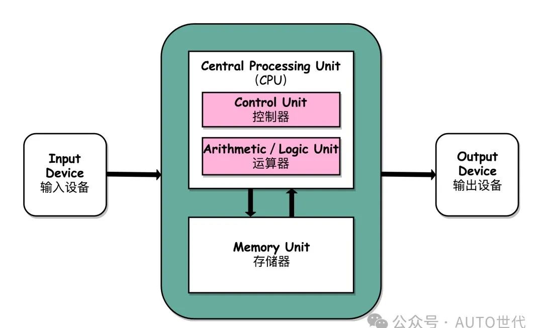
─ Control Unit): Directs the ALU to work in an orderly manner, including fetching instructions from memory, translating instructions, analyzing instructions, and then sending control commands to relevant components based on the instructions to control the execution of the operations contained in the instructions.
─ Memory Unit): A hardware component used to store data and program instructions. Depending on its location and characteristics, it can be further divided into internal memory, external memory, random access memory (RAM), and read-only memory (ROM), etc.
Among them, the arithmetic and control units are integrated in the CPU, thus the CPU is born.
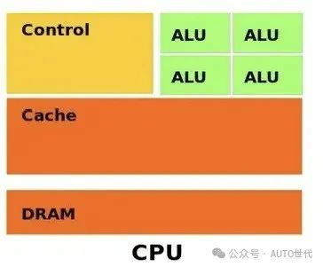
Since the CPU must have extremely high versatility to handle various types of data and needs to perform logical judgments, this introduces a large number of branch jumps and interrupt handling, making the internal structure of the CPU extremely complex. Because of this, the number of ALU units inside the CPU is actually very limited, with most of the space occupied by the control unit and Cache. To increase the possibility of parallel computing, the CPU can adopt a multi-core structure, such as dual-core, quad-core, hexacore, etc., but the number will not be too many!
In the CPU memory system, there is an important concept called cache, which is used to reduce the time required for the CPU to access DRAM. The cache is a smaller memory area but with faster access speed, located closer to the processor core, used to store copies of data from DRAM. Cache is usually divided into multiple levels, typically including three levels: L1, L2, and L3. The closer the cache is to the core, the smaller its capacity but the faster its speed. For example, L1 cache might be 64KB, L2 cache 256KB, and L3 cache 4MB.
The basic workflow is shown in the figure below:
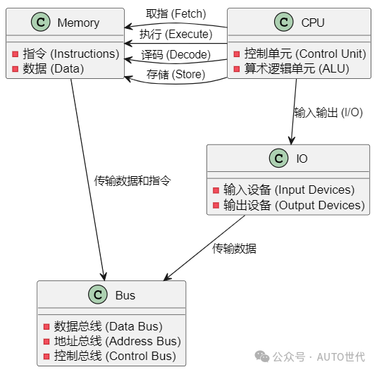
In addition, to increase computational efficiency, the CPU adopts the MIMD (Multiple Instruction, Multiple Data) working mechanism. Simply put, MIMD is like various departments in a large company, where each department (processor) independently handles different tasks (instructions) and data, improving overall efficiency through parallel work. This mechanism allows the system to handle multiple tasks simultaneously, flexibly responding to different needs, but it also requires effective management to coordinate resources and tasks to ensure smooth operation.
1. Von Neumann Bottleneck: Due to the sharing of the same bus for instructions and data, the CPU needs to go through the same bus every time it reads instructions and data, causing performance bottlenecks.
02
MCU: Automotive Embedded Solutions
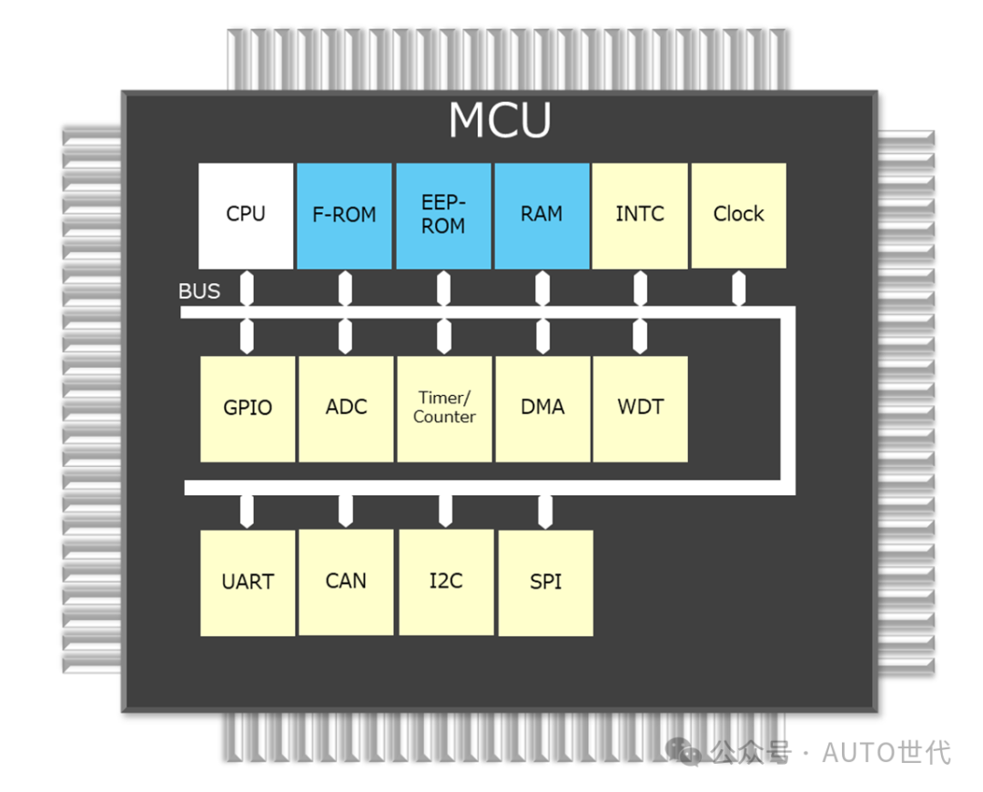
MCU (Micro Controller Unit), also known as a microcontroller or single-chip microcomputer, is a microcomputer that integrates multiple functional modules, including CPU, memory (ROM/RAM), data converters (A/D, D/A), input/output interfaces (I/O), and timers.
2. High Performance and Low Power Consumption: With the increase in automotive electronic functions, MCUs need to process more data and execute more complex computational tasks. Therefore, automotive-grade MCUs need to have high-performance computing capabilities while also maintaining good control over power consumption to meet the demands of automotive battery power supply.
4. Real-Time Performance: In autonomous driving and advanced driver-assistance systems (ADAS), MCUs need to respond to various sensor data in real-time and make decisions. Therefore, automotive-grade MCUs typically need to have strong real-time processing capabilities and low-latency performance.
Additionally, to achieve hard real-time, high reliability, and safety in automotive control systems, and to make software development and integration across different MCU platforms more efficient and portable, AUTOSAR (Automotive Open System Architecture) has emerged, which is also a unique product of automotive MCUs.
AUTOSAR introduces a hardware abstraction layer, allowing upper-layer software to be independent of specific MCU hardware, and through standardized interfaces and services, AUTOSAR enables application software to run on different MCU platforms, requiring only adaptation of the underlying drivers. However, it is still largely monopolized by foreign suppliers, and the cost of development toolchains is extremely high. Although more and more non-AUTOSAR software architectures are being applied for intelligent driving systems, AUTOSAR still holds an unshakable position in traditional hard real-time and high safety requirement control systems!
03
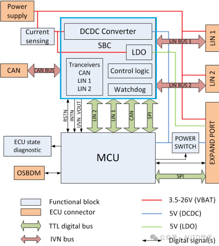
SBC: Safety Monitoring Solutions
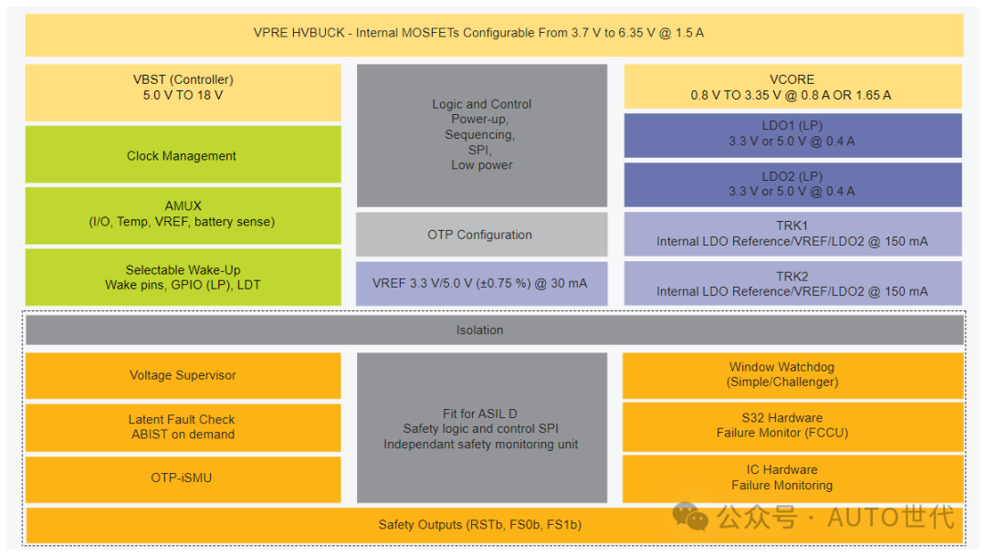
Therefore, in functional safety monitoring architectures, including the classic three-layer E-Gas architecture, SBC chips often serve as independent monitoring chips, monitoring the main MCU and providing watchdog, interrupt, and other services, as shown in the figure below:
In Conclusion:
The chip series, decoding the content related to automotive processors CPU, MCU, SBC, is now complete , and I hope it can provide friends with a better understanding.
Further Reading

▼Click the book cover to learn more
“Functional Safety of Automotive Systems Based on ISO26262 – Methods and Practices””
Series Name: Automotive Technology Boutique Series

▼Click the book cover to learn more

Compiled by the Automotive Chip Industry Innovation Strategic Alliance, Research Group on Automotive Chip Standard System Construction
Recommendation: Compiling automotive chip standardization direction steps by concentrating industry strength.

▼Click the book cover to learn more
“Functional Safety Based on ISO26262”
Recommendation: Hands-on guidance for readers on learning functional safety management through specific projects, making the dull and monotonous functional safety standards more concrete and vivid.

▼Click the book cover to learn more
Series Name: Automotive Technology Innovation and R&D Series
Authors: Guo Jian, Wang Gaohong, Zhao Yongxin, Pu Guoguang

END
Image Source: Auto Generation
Image Production: Dong Chunhui
Editor: Sun Peng
Reviewer: Zhang Ping