This article is reprinted from the public account: Software-Hardware Integration (ID: cash-arch)
Editor’s Note
Recently, the National Development and Reform Commission and four other departments jointly released the “Implementation Plan for the National Integrated Big Data Center Collaborative Innovation System Computing Power Hub,” proposing to build national computing power network hub nodes in Beijing-Tianjin-Hebei, Yangtze River Delta, Guangdong-Hong Kong-Macao Greater Bay Area, Chengdu-Chongqing, as well as Guizhou, Inner Mongolia, Gansu, and Ningxia, and to launch the “Eastern Data for Western Computing” project to construct a national computing power network system.
Computing power has become the key to the development of the entire digital information society. The “Eastern Data for Western Computing” can alleviate some problems, but it does not fundamentally solve them: currently, to enhance computing power, it relies more on the “spreading the cake” method to build larger and low-energy modern data centers.
This is the Scale out (increasing scale) of computing power. So, how can we achieve Scale up (enhancing the performance of individual computing nodes) of computing power? In other words, how can we significantly (by orders of magnitude) improve the performance of a single processor?
Currently, computing power has become the core issue restricting the more vigorous development of information technology:
-
CPUs have good flexibility but the lowest efficiency and have already reached a performance bottleneck;
-
GPUs have certain flexibility, but their efficiency is still inferior to DSA, and they will soon face performance bottleneck issues similar to CPUs in the foreseeable future.
-
DSA offers some flexibility under extreme performance conditions. However, the various and rapidly changing domain applications have not yet achieved large-scale implementation of DSA chips.
We need to build a new generation of innovative computing paradigms that can enhance computing power by at least 1-2 orders of magnitude compared to the current level and provide excellent programming capabilities to continuously meet the challenges of the explosive demand for computing power in more complex systems over the next ten years.

1 First Generation: CPU
1.1 Instruction Set Software-Hardware Decoupling, CPU Performance Soars, Software Flourishes
The instruction set is the medium between software and hardware. The CPU is the most flexible because the instructions executed on the CPU are primarily basic arithmetic operations, along with some memory access and control instructions, like building blocks that can be freely combined to create various functional forms, resulting in complex and powerful programs, or software.
The greatest value of the CPU lies in providing and standardizing an instruction set that decouples software from hardware:
-
Hardware engineers do not need to care about the scenarios, only focusing on rapidly improving CPU performance through various “extreme means”.
-
Software engineers, on the other hand, do not need to consider hardware details, only focusing on the program itself. With the support of high-level programming languages/compilers, operating systems, and various system frameworks/libraries, a huge software ecosystem super empire has been built.
Through the standardized instruction set, software and hardware are decoupled and can be forward compatible (software can be forward compatible with previous hardware, and hardware can be forward compatible with previous software). Thus, CPU hardware designers do not need to consider what the upper-level business is, meaning they do not care about what the program composed of instruction combinations does. They only need to care about how well their designed CPU performs, achieving higher IPC (Instructions per Cycle) and higher frequency.
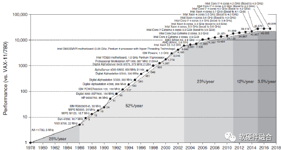
Figure 1 Comparison of CPU Performance Improvement Over the Years
From Figure 1, it can be seen that over nearly 40 years, the overall performance of CPUs has increased by nearly 50,000 times. On one hand, this is due to the revolutionary changes in processor architecture and advances in semiconductor technology. On the other hand, it is also due to the standardized instruction set, which decouples the hardware implementation of the CPU platform from software programming, allowing both to flourish without the constraints of the other.
On one hand, CPU performance is soaring, while on the other, software has gradually developed into a super ecosystem. From various high-level programming languages with millions of users to widely used intelligent operating systems in cloud computing data centers, PCs, mobile phones, etc., to various specialized databases, middleware, and cloud computing foundations such as virtualization and containers, all these software are foundational support software, representing the “tip of the iceberg” of software, while more are various user-level application software, system-level and application software, jointly forming a software super ecosystem based on CPUs.
1.2 Moore’s Law Failure, CPU Performance Bottleneck, Restricting Software Development
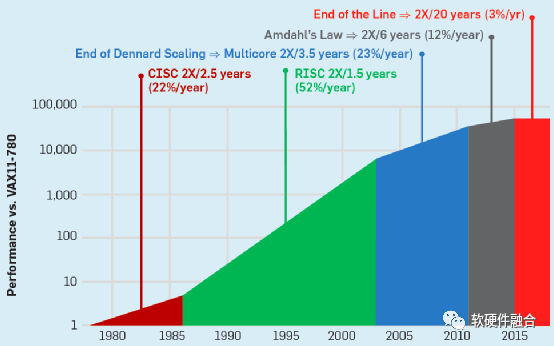
Figure 2 Five Stages of CPU Performance Improvement
Figure 2 is consistent with Figure 1 from the previous section, primarily clarifying the five stages of development:
-
CISC Stage. In the 1980s, the CISC architecture CPU, represented by Intel and AMD’s x86 architecture, opened the era of rapid performance improvement for CPUs, with CPU performance increasing by about 25% annually (the 22% data in the figure is incorrect), doubling approximately every three years.
-
RISC Stage. Subsequently, CISC systems became increasingly complex, with many design resources spent on implementing infrequently used instructions. RISC proved that “the more streamlined, the more efficient.” With the rise of RISC architecture CPUs, performance improvement accelerated further, reaching 52% annually, with a doubling time of only 18 months.
-
Multi-Core Stage. As the performance improvement of single-core CPUs became increasingly difficult, the approach of integrating more CPU cores in parallel began to enhance performance further. During this period, the performance improvement could reach 23% annually, with a doubling time of 3.5 years.
-
Multi-Core Overall Performance Diminishing Stage. As the number of integrated CPU cores increased, Amdahl’s Law proved that the benefits brought by increasing the number of processors would gradually diminish. During this period, CPU performance improvement was only 12% annually, with a doubling time of 6 years.
-
Performance Improvement Bottleneck Stage. When various means such as architecture/microarchitecture design, process, and multi-core parallelism have been exhausted, the overall performance improvement of CPUs reaches a bottleneck. As shown in the figure, since 2015, CPU performance improvement has only been 3% annually, with a doubling time of 20 years.
2 Second Generation: GPU
2.1 GPGPU, A General-Purpose Parallel Computing Platform
GPU, Graphics Processing Units. As the name suggests, GPUs are specialized accelerators primarily used for graphics processing. The internal processing of a GPU is supported by many parallel computational units. If used solely for graphics processing, it would be a waste of resources, as its application range is too narrow.
Therefore, the internal computational units of the GPU were generalized and redesigned, turning the GPU into a GPGPU. By 2012, GPUs had evolved into highly parallel multi-core systems, with GPGPU possessing powerful parallel processing capabilities and programmable pipelines, capable of processing both graphical and non-graphical data. Especially when facing SIMD-type instructions, the computational workload for data processing far exceeds that for data scheduling and transmission, GPGPU significantly outperforms traditional CPU applications. The GPUs we refer to today usually mean GPGPU.
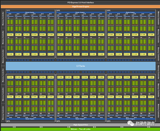
Figure 3 NVIDIA Turing GPU Architecture
In 2018, NVIDIA released the latest generation of GPU architecture—the Turing architecture. The GPUs based on the Turing architecture provide PCIe 3.0 to connect to the CPU host interface and offer gigabit thread engines to manage all workloads. Additionally, the Turing architecture supports data consistency access between multiple GPUs via dual x8 NVLink interfaces.
As shown in Figure 3, the core processing engine of the Turing architecture GPU consists of the following parts: 6 Graphics Processing Clusters (GPC); each GPC has 6 Texture Processing Clusters (TPC), totaling 36 TPCs; each TPC has 2 Streaming Multiprocessors (SM), totaling 72 SMs. Each SM consists of 64 CUDA cores, 8 Tensor cores, 1 RT core, and 4 texture units, totaling 4608 CUDA cores, 576 Tensor cores, 72 RT cores, and 288 texture units.
2.2 CUDA, The Key to NVIDIA’s Success
Figure 4 CUDA Framework
In 2006, NVIDIA launched CUDA, a general-purpose parallel computing platform and programming model that utilizes the parallel computing engine within NVIDIA GPUs to solve many complex computing problems more efficiently than CPUs. CUDA provides developers with a software environment using C++ as a high-level programming language. It also supports other languages, application programming interfaces, or instruction-based methods, such as FORTRAN, DirectCompute, and OpenACC.
CUDA is key to NVIDIA’s success, greatly lowering the barrier for users to engage in GPU parallel programming. On this basis, powerful development libraries and middleware have been built for different scenarios, gradually establishing a strong ecosystem of GPU + CUDA.
3 Third Generation: DSA
3.1 The Rise of DSA
In March 2017, Turing Award winners David Patterson and John Hennessy proposed the DSA architecture in their keynote speech titled “The Golden Age of Architecture.” The performance improvement of CPUs is reaching its end, and targeted customization acceleration for specific scenarios is needed, which DSA provides a feasible solution. DSA is a callback based on customized ASICs, giving them a certain degree of software programmability.
According to the “complexity” of instructions, DSA can be classified as ASIC. Compared to CPUs, GPUs, FPGAs, and traditional ASICs, DSA has the following characteristics:
-
Similar to GPUs and FPGAs, typical DSAs are not Turing complete. They are designed for compute-intensive tasks in the system rather than running the entire system. Therefore, the architecture of DSA platforms is “CPU + DSA”. -
DSA has a simple instruction set and is programmable, thus it is a processor; DSA is custom-designed for specific domains, making it a special type of ASIC. DSA can be seen as a return from traditional ASICs to general-purpose processing, increasing the flexibility of ASICs. -
If the scale of DSA application areas is large enough, IC chips can be customized to cover the high upfront costs of IC chips; if the scale is smaller, choosing FPGA to implement DSA design is a better option. -
Architecture and logic design need to understand specific domains and relevant algorithms, rather than focusing solely on architecture and design itself. -
Heterogeneous programming based on CPU + DSA is a significant challenge.
3.2 DSA Case in AI: Google TPU
The first classic case of DSA architecture is Google’s TPU. TPU (Tensor Processing Unit) is a custom ASIC chip developed by Google to accelerate machine learning workloads. A predictive analysis conducted by Google in 2013 indicated that people use voice recognition DNN for voice search for three minutes daily, which would double the computing needs of data centers, making traditional CPU costs prohibitively expensive. Therefore, Google launched a high-priority project, the TPU project, to quickly generate self-developed ASICs for inference, aiming to improve the cost-effectiveness of GPUs by tenfold.
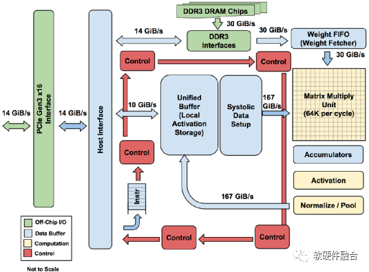
Figure 5 Structure Diagram of Google TPU 1.0
As shown in Figure 5, the TPU instruction is sent from the Host to the TPU’s instruction buffer via PCIe Gen3 x16 bus. Internal modules are connected via a 256-byte wide bus. Starting at the top right corner, the matrix multiplication unit is the core of the TPU, containing 256×256 MACs capable of performing 8-bit multiply-accumulate operations on signed or unsigned integers, with 16-bit products collected in 4 MB 32-bit accumulators located below the matrix unit. The 4 MB can hold 4096 accumulators of 256 elements each. The matrix unit generates a partial sum of 256 elements every clock cycle.
TPU instructions are designed as CISC (Complex Instruction Set Computing) type, including a repeat domain. The CPI (Cycles per Instruction) of these CISC-type instructions typically ranges from 10 to 20. There are approximately twelve instructions in total, with the five main instructions being:
-
Read_Host_Memory. Reads data from CPU memory into the Unified Buffer (UB).
-
Read_Weights. Reads weights from weight storage into the weight FIFO as input for the matrix unit.
-
MatrixMultiply / Convolve. Directs the matrix unit to perform matrix multiplication or convolution from the Unified Buffer to the accumulators. Matrix operations use variable-sized B*256 inputs, which are then multiplied by 256×256 constant weight inputs to generate B*256 outputs, requiring B pipeline cycles to complete.
-
Activate. Executes non-linear functions of artificial neurons based on options like ReLU, Sigmoid, etc. Its input is the accumulator, and its output is the Unified Buffer. When connected to non-linear function logic, dedicated hardware on the chip can also be used to perform pooling operations required for convolution.
-
Write_Host_Memory. Writes data from the Unified Buffer back to CPU memory.
Other instructions include auxiliary Host memory read/write, group configuration, two versions of synchronization, interrupting the host, debugging tags, no-operation (NOP), and halt.
(★ represents TPU, ▲ represents K80 GPU, ● represents Haswell CPU)
Figure 6 Roofline Plot of CPU, GPU, and TPU
As shown in Figure 6, for HPC, the Y-axis represents the performance of floating-point operations per second, while the X-axis measures operational intensity in floating-point operations per DRAM byte accessed. The peak computing rate corresponds to the “flat” part of the Roofline, while memory bandwidth is measured in bytes per second, forming the “sloped” part of the Roofline. From Figure 6, we can see that all TPU stars are located above the Roofline of both CPU and GPU. The flat part of the Roofline indicates that the TPU’s processing speed is 15-30 times faster than that of GPUs and CPUs.

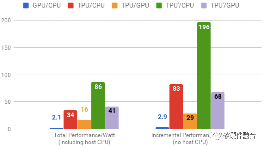
Figure 7 Performance-Power Ratio of CPU, GPU, and TPU
As shown in Figure 7, the TPU’ uses GDDR5 memory and is an improved version. It can be seen that compared to CPUs, the performance increases by 196 times, and compared to GPUs, it increases by 68 times. Google subsequently developed TPU 2.0 and 3.0 versions. TPU 1.0 achieved a peak performance of 92 Tops, while TPU 2.0 reached 180 Tflops, and TPU 3.0 further achieved 420 Tflops. Moreover, starting from TPU 2.0, TPU is no longer used as an acceleration card for general servers but as a customized TPU cluster, maximizing the acceleration value of TPU.
3.3 DSA Case in Networking: Intel Tofino
With the rapid development of SDN, from the control plane programmable OpenFlow to the data plane programmable P4 language, the Intel PISA architecture Tofino chip has emerged. From an architectural perspective, Tofino is the most typical DSA in the networking field, as its implemented programmable pipeline can achieve ASIC-level performance while allowing programming of the entire packet processing data plane via P4.
Intel designed an ASIC switch chip for data centers based on the PISA architecture, supporting P4 data plane programming. The goal is to make network programming as simple as CPU programming. When the network is fully programmable (i.e., both the control plane and data plane are under the final user’s control), the networking industry will enjoy rapid development akin to software.
In Intel’s view, although NPUs and FPGAs exist, allowing modification of network protocols and editing of data packets while providing moderate programmability for those who know how to write microcode or RTL, their performance does not match that of ASICs. Therefore, NPUs and FPGAs can only find their place in performance-insensitive areas. Intel provides a win-win solution for the networking industry: a programmable data plane protocol that achieves the highest industry speeds. Intel has developed the world’s first programmable switch chip faster than traditional ASICs, making network programming easy and universal.
Intel collaborated with Google, Microsoft, Princeton, and Stanford to develop an open-source network programming language P4. Programmers can program once based on P4 to describe network behavior, then compile the program to run on various platforms. P4 offers differentiated means for network device manufacturers and network owners, allowing their products or entire networks to perform better than competitors.
This stands in stark contrast to the current situation where, if users want to add new features to the network, they must share that feature with chip suppliers and see it appear in competitors’ networks, defeating the purpose of differentiation. Device manufacturers are also reluctant to add new features, as doing so can take years and the competitive advantage is often fleeting. This has led some companies to prefer developing proprietary fixed-function ASICs to maintain their lead.
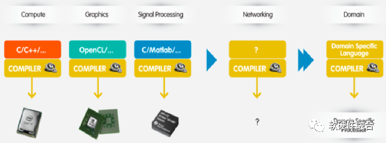
Figure 8 Network Compiler Like CPU Compiler
As shown in Figure 8, programmability has long existed in computing, graphics, digital signal processing, and specific domain processors, enabling a thriving developer community to innovate rapidly and write end-user-centric solutions. Intel’s PISA architecture allows complete control to be handed over to network owners, similar to DSPs, GPUs, and TPUs.
To achieve this, Intel first identified a small-scale primitive instruction set for packet processing, totaling about 11 instructions. It also established a highly unified programmable pipeline (PISA architecture) to rapidly and continuously process packet headers. Programs are written in the domain-specific language P4, then compiled by Intel’s Capilano compiler, optimized to run at line speed on PISA architecture devices. Intel aims to make networks more agile, flexible, modular, and cost-effective.
Intel believes that network systems are developing towards a three-layer structure: at the bottom is a P4 programmable Tofino switch, above it is a Linux-based operating system running proprietary control plane applications. Intel provides the industry with the fastest, most programmable, P4-optimized switch hardware.
4 Fourth Generation: CASH Ultra-Heterogeneous
4.1 Chips from 2D to 3D to 4D, Increasing Number of Transistors per Chip
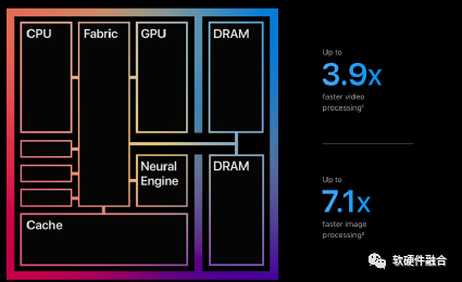
Figure 9 Apple M1 Chip Description
As shown in Figure 9, Apple’s self-developed ARM CPU M1 is based on TSMC’s 5nm process and contains 16 billion transistors. Such a large-scale design allows the M1 to integrate an 8-core CPU and an 8-core GPU, with each processor being able to lavishly utilize internal Register, Buffer, or Cache resources (which consume a lot of transistors).
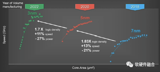
Figure 10 TSMC New Process Roadmap
As shown in Figure 10, TSMC’s 5nm has just entered mass production, while its 3nm process is already on the way, with 2nm and 1nm also on the roadmap for the next few years. Moreover, TSMC has begun tackling the 0.1nm process, and semiconductor processes are about to enter the sub-nanometer (angstrom) era.
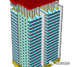
Figure 11 3D Storage Packaging
As shown in Figure 11, in recent years, 3D packaging technology has emerged in the storage field, allowing integrated circuits to transition from two-dimensional to three-dimensional.
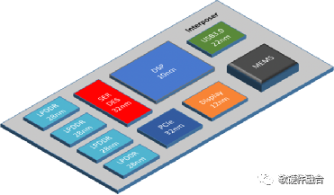
Figure 12 Chiplet Schematic
As shown in Figure 12, the chiplet mechanism integrates multiple chip bare dies together, enhancing the transistor integration density per unit area from 3D to 4D.
Continuous process advancements, 3D stacking, and chiplet multi-die interconnection have allowed chips to evolve from 2D to 3D to 4D. These technological advancements mean that more transistors can fit within the scale of a chip, leading to larger chip sizes.
4.2 From Heterogeneous to Ultra-Heterogeneous, From SOC to Multi-SOC, Increasing Design Scale
(a) CPU Homogeneous Parallel (b) CPU + xPU Heterogeneous Parallel
Figure 13 Homogeneous Parallel and Heterogeneous Parallel Computing Architectures
Currently, the mainstream architectures of parallel computing are shown in Figure 13:
-
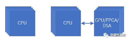
Figure 13(a) represents CPU homogeneous parallelism. Common multi-core CPUs and multi-CPU socket interconnections are examples of homogeneous parallel computing. Due to its good flexibility and generality, the CPU is the most common parallel computing architecture. However, as the performance of individual CPU cores has reached a bottleneck, and the number of CPU cores that can fit on a single chip is also nearing its limits, there is little room left for performance optimization in CPU homogeneous parallelism.
-
Figure 13(b) represents CPU + xPU heterogeneous acceleration parallel architecture. Generally, GPUs, FPGAs, and DSA accelerators exist as co-processing accelerators to the CPU, but they are not Turing complete. Therefore, these accelerators require control from the CPU, making CPU + xPU a typical architecture.
The situation of heterogeneous parallel computing architectures is as follows:
-
If the CPU does not participate in computing, and is responsible for controlling GPUs and other accelerators as well as coordinating tasks and data, then a particularly powerful CPU is not necessary. The overall computing performance of the entire heterogeneous computing is mainly determined by the accelerators.
-
As an accelerator, GPUs have certain flexibility, but their efficiency is still inferior to DSA, and they will soon face performance bottleneck issues similar to CPUs in the foreseeable future.
-
FPGAs as accelerators are typically used as FaaS platforms, fully utilizing the flexible programmability of FPGA hardware, constrained by their programming difficulty and design scale.
-
DSA as an accelerator provides some flexibility under extreme performance conditions. However, the various and rapidly changing domain applications have not yet achieved large-scale implementation of DSA chips.
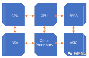
Figure 14 Ultra-Heterogeneous Parallel Computing with Multiple Processing Engines Coexisting
As the design scale supported by chip processes continues to grow, CPUs, GPUs, FPGAs, and specific algorithm engines can all be integrated as IP into larger systems. Thus, building a larger-scale chip design becomes possible. Here, we propose the concept of “ultra-heterogeneous” parallel computing, as shown in Figure 14, referring to a complex chip system composed of CPUs, GPUs, FPGAs, DSAs, ASICs, and various other processor engines.
From a system perspective, traditional SOCs are single systems, while ultra-heterogeneous systems integrate multiple systems into a larger macro system. The differences and connections between traditional SOC and ultra-heterogeneous SOC are:
-
Difference in design scale. MCU chips are SOCs, mobile phone chips are SOCs, and ultra-heterogeneous architecture chips are also SOCs. So where is the difference? However, MCU-level SOCs generally do not run operating systems or run RTOS-level operating systems for simple control and processing. Mobile phone SOCs need to run large operating systems like Android and iOS, making our phones increasingly resemble computers. The ultra-heterogeneous architecture, however, does not simply run operating systems and various software, but focuses on providing a large resource pool that is both powerful and can be flexibly and fully utilized by software; with the assistance of lower-level software, it transforms hardware into a neutral computing platform resource pool, allowing software to partition and combine computing power more flexibly for users.
-
Single system versus multiple systems. Traditional SOCs typically have a core control program based on the CPU to drive the operations of the CPU, GPU, peripheral modules, and interface data I/O. The operation of the entire system is centrally managed and controlled. In contrast, due to the scale and complexity of ultra-heterogeneous systems, it is challenging to achieve this. Each subsystem is essentially a traditional SOC-level system that needs to interact based on specific protocols. The entire ultra-heterogeneous system exhibits characteristics of a distributed system.
-
Data flow-driven versus instruction flow-driven. In traditional SOCs, the CPU operates based on instruction streams (programs), and then the CPU drives the GPU and other acceleration modules and I/O modules. In ultra-heterogeneous multi-SOC systems, due to the complexity of the systems, it is difficult to synchronize control interactions between different systems through instruction flow design patterns. The entire interaction is actually driven by data interactions. Moreover, due to the drastic increase in the bandwidth of data to be processed, many processing engines operate in a data flow-driven manner rather than an instruction flow-driven manner. This can be understood as data flow driving the operation of the entire macro system.
Ultra-heterogeneous systems need to achieve performance improvements of 10 to 100 times or more compared to traditional GPU or DSA-based heterogeneous computing, while also achieving extreme performance close to that of ASICs, and ensuring that the entire system approaches the general programmability level of CPU software.
4.3 Software-Hardware Integration, The Only Path for Ultra-Heterogeneous Computing
With the development of cloud computing, data centers have reached ultra-large scales, with each ultra-large data center housing tens of thousands or even hundreds of thousands of servers. The development of ultra-large data centers is the fundamental driving force for cloud computing gradually moving towards software-hardware integration.

Figure 15 Software-Hardware Integration and Continuous Offloading of CPU Systems
The various software running on cloud servers can be seen as a very complex and layered system. Due to the performance bottleneck of CPUs, under the macro-scale of data centers, and some services optimized for specific scenarios at the IaaS layer, as shown in Figure 15, we can consider that the process of software-hardware integration is essentially a process of continuous offloading of the system.
Software-hardware integration:
-
Does not change the system hierarchy and component interaction relationships, but breaks the boundaries between software and hardware, achieving overall optimization through system-level collaborative design.
-
Traditional layers are clear, with hardware at the bottom and software at the top; in software-hardware integration, each task module can be software, hardware, or a combination of both. There is software within hardware, and hardware within software, blending into a unified whole.
-
From a macro perspective, the higher the layer, the more flexible the software components, while the lower the layer, the more fixed the hardware components. The enormous scale and specific scenario services have led to the gradual stabilization of the cloud computing bottom layer workload, which is progressively offloaded to hardware (a passive trend).
-
The software-hardware integrated architecture makes “hardware” more flexible and powerful, allowing more functional layers to shift towards “hardware” acceleration (an active trend).
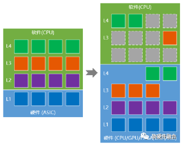
Figure 16 DPU Implemented Based on CASH Architecture for Ultra-Heterogeneous
Typically, we consider DPU as an acceleration for offloading tasks from the CPU, but this idea still does not escape the constraints of CPU-centric architecture design.
More fundamentally, as shown in Figure 16, the DPU based on the CASH architecture (CASH, Converged Architecture of Software and Hardware) is a powerful, fully functional ultra-heterogeneous computing power platform. This platform includes hardware acceleration parts to complete the acceleration processing of the underlying infrastructure layer; it also includes CPUs and GPUs for application layer processing.
Independent CPUs and GPUs can be seen as extensions of the DPU, only utilized as independent computing platforms to enhance the overall system’s functionality when the integrated CPU/GPU cannot meet processing requirements.
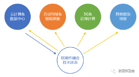
Figure 17 Software-Hardware Integration Technology as the Foundation for Various Complex Computing Scenarios
Software-hardware integration technology has gradually formed as a technical concept and a complete set of technical systems to address the most complex challenges in cloud computing data centers, which have the highest computing power demand, largest system scale, most sensitive costs, and highest flexibility requirements.
Based on software-hardware integrated ultra-heterogeneous hybrid computing, the focus is on increasing computing power by 1-2 orders of magnitude for complex scenarios. Looking ahead, scenarios such as autonomous driving, 5G/6G core networks, and edge computing will have even stronger demands for computing power. In the face of so many complex system scenarios, software-hardware integration will have more applications.
As shown in Figure 17, software-hardware integration abstracted from cloud computing guides the chip and system design of complex system scenarios, including cloud computing and autonomous driving.
5 Conclusion
Software-hardware integrated ultra-heterogeneous computing needs to meet the following standards:
-
Performance. The performance level per unit transistor resource should be close to that of ASICs, and overall performance needs to reach 10-100 times or more compared to GPGPU and DSA.
-
General Flexibility. On the premise of ensuring extreme performance, its programmability must approach that of CPU software. Additionally, it should provide developers with a user-friendly programming platform.
-
Openness and Open Source. The three main architecture platforms for CPUs are x86, ARM, and RISC-V, while the DSA aspect is defined by various incompatible architectures from different companies. In the ultra-heterogeneous era, under the support of software-defined systems, an open, standardized architecture definition is essential for achieving true “interconnectivity” between different architectures and software ecosystems.
The computing power and versatility of each platform are summarized in Figure 18.
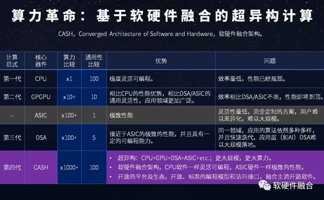
Figure 18 Comparison of Computing Power Platforms: CPU, GPU, DSA, CASH
(End of text)
Editor: Lu Dingci