The new year’s innovation competition is in full swing~
To help everyone better understand this event, the editor has organized excellent works from 2021 for learning and sharing.
Every Monday, we will share award-winning works, so remember to check out the series! ~
Team Introduction
Participating Unit: Shanghai University of Electric Power Team Name: Haixing Team Final Award: Second Prize
1. Abstract
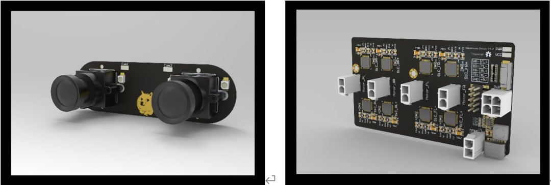
With the development of information technology, **Automated Guided Vehicles (AGV)** have been widely used in scenarios such as **intelligent manufacturing** and **smart logistics**. The navigation system of AGV vehicles mainly utilizes sensors such as vision and **LiDAR**, and its main control system often employs multiple chips and complex embedded systems, leading to high costs, large power consumption, and poor real-time performance. To address these issues, this design builds an **ARM-M3 soft core** on the Xilinx FPGA platform, designing an SOC and related control peripherals that accelerate dual-camera disparity image computation, validating the basic functionality of guiding AGV vehicles with a single chip. The main work of this design is reflected in the following aspects: 1) An **ARM-M3 microprocessor** and related peripherals were constructed on the Xilinx Artix XC7A200T platform. Images were collected using an **OV5640 dual-camera**, accelerated by a co-processor, and the ARM-M3 microprocessor analyzed the surrounding environment for path planning, ultimately generating PWM signals to drive the vehicle’s movement. 2) On the hardware side, this design custom-built the **OV5640 dual-camera** and **SiC780 silicon carbide motor driver board**. By analyzing the principles of dual-camera vision, the custom dual-camera adopted a parallel dual-stereo vision mode as the design scheme. Thanks to the **Mecanum wheels** used by the vehicle for omnidirectional movement and the custom high-current silicon carbide driver board, the vehicle can move freely and flexibly. 3) On the algorithm side, this design performed parallel optimization on traditional stereo matching algorithms, greatly improving the algorithm’s running speed and ultimately achieving a good balance between resource consumption, power consumption, and running speed. To eliminate radial distortion, tilt distortion, and tangential distortion in images, this design used the Zhang Zhengyou calibration method to calibrate and correct the dual-camera. The internal and external parameters of the camera were obtained using Matlab’s automatic calibration tool, the **Stereo Camera Calibrator App**, and incorporated into the correction algorithm to finally achieve image correction. 4) In testing, this paper analyzed the problems of excessive time consumption in feature matching and high error rates in traditional stereo matching algorithms, conducting comparative experiments on Raspberry Pi 3B and PC. 5) In application scenarios, video data was collected to build a QR code dataset, and **TensorFlow** was used to train a fixed-point convolutional neural network, utilizing **HLS** to construct a CNN IP core, enabling QR code detection capabilities.
2. System Function Introduction
2.1 Overall Introduction
The goal of this work is to design an SOC for AGV vehicles based on the ARM Cortex-M3 DesignStart RTL Eval processor IP provided by ARM, developing a dual-camera depth vision co-processor capable of sensing obstacles.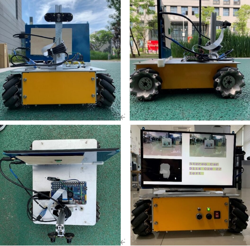
Design content includes:
-
Developed a dual-camera stereo matching smart co-processor based on the **BM (Block Matching)** algorithm;
-
Designed and manufactured the **OV5640 dual-camera circuit board**, and dual-camera video acquisition **Verilog driver IP**;
-
Designed an LCD driver for displaying parameters and images;
-
Designed and manufactured a motion control module driver board and related PWM drivers;
-
Controlled a **Mecanum vehicle** with omnidirectional movement capability for obstacle avoidance demonstration.
-
Constructed a CNN IP core to enable QR code detection capabilities.
2.2 System Flow
This system constructs an **ARM Cortex-M3 processor** on the Xilinx FPGA Artix XC7A200T, paired with a self-designed **OV5640 dual-camera** to collect video and store it in DDR using **VDMA**. The depth acceleration module performs distortion correction and stereo matching based on the camera calibration parameters and caches the resulting disparity map. The M3 soft core reads the disparity map from DDR, calculates the relative distance to obstacles ahead, and performs path planning. Finally, the frame rate data is read, and the camera image, disparity results, movement direction, and image frame rate are displayed on the LCD, controlling the vehicle according to the planned results.
3. System Architecture
3.1 Architecture Overview
The system is mainly composed of four modules: video acquisition, image processing, real-time display, and motion control.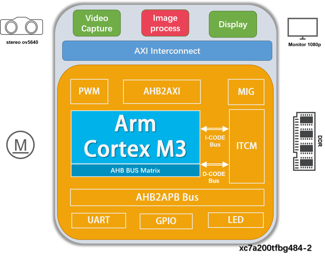 A, Video Acquisition Module consists of three sub-modules: camera acquisition, register configuration, and video stream conversion, achieving configuration of the resolution and imaging parameters of the self-designed dual-camera and transmitting the collected data to the image processing module. B, Image Processing Module connects the VDMA, frame rate counter, depth acceleration core, and OSD result presentation through an AXI connector configured for high-performance mode, realizing disparity map calculation and frame rate counting functions, which are finally summarized and passed to the display module for display. C, Display Module consists of video stream conversion, video timing controller, dynamic clock, and VGA display, constructed based on the high-performance video system reference design structure and parameter configuration. The video timing controller generates line and field synchronization signals corresponding to 1080p and outputs them to the VGA display module through the video stream conversion sub-module, with a dynamic clock configurable by the user to drive the VGA display module for adaptation to different screen resolutions. Under the cooperation of these modules, images with a resolution of 1080p and a refresh rate of 60Hz are displayed along with running parameters. D, Motion Control Module mainly consists of ARM-M3 core, UART, GPIO, and PWM sub-modules. The M3 core reads the results from the depth acceleration module in DDR for simple calculations, estimating the distance to obstacles ahead for path planning. Finally, it outputs the frame rate data from the video acquisition module and depth output module along with the vehicle’s running direction to the result presentation module and UART serial port, achieving real-time presentation of operating parameters.
3.2 Software and Hardware Function Division
Compared to traditional microcontrollers that serially collect camera data and transmit single pixels for display, the stable disparity map calculations that are difficult to achieve on PCs are implemented by hardware in this system, greatly reducing the CPU load. The software part is mainly implemented in **Keil** using **C language**, primarily for initializing various peripherals and configuring camera registers. After initialization, frame rate counting module data and depth acceleration module results are read, and simple arithmetic operations are performed according to formulas to complete distance estimation. Based on the estimated results, PWM and display module registers are configured to achieve motion control and real-time display.
3.3 Peripheral Mounting
The central processing unit of this system is the ARM Cortex-M3 DesignStart RTL Eval provided by ARM, with the entire system and peripherals deployed on the **Xilinx xc7a200tfbg484 FPGA platform**. The system mainly consists of the Cortex-M3 soft core, **OV5640 dual-camera module**, depth acceleration module, DDR3 memory controller, VGA display, AHB bus matrix, AXI bus, and APB low-speed peripherals, as shown in the detailed block diagram below.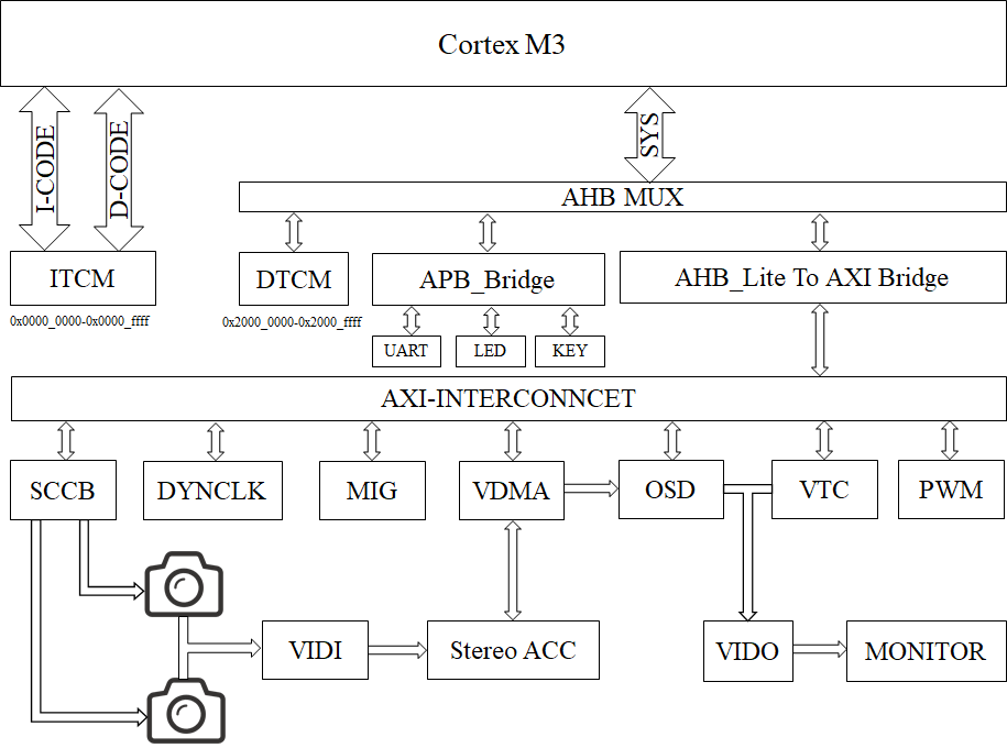
4. Module and System Function Simulation and Testing
4.1 Camera Test Simulation
The register configuration of the **OV5640 camera** is controlled by the M3 soft core through GPIO simulating SCCB. A **DSLogic** logic analyzer is used to capture pin levels, and its accompanying software **DSView** can parse IIC protocols compatible with SCCB, displaying the commands and data corresponding to different level combinations.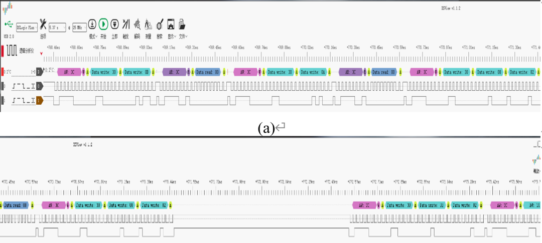
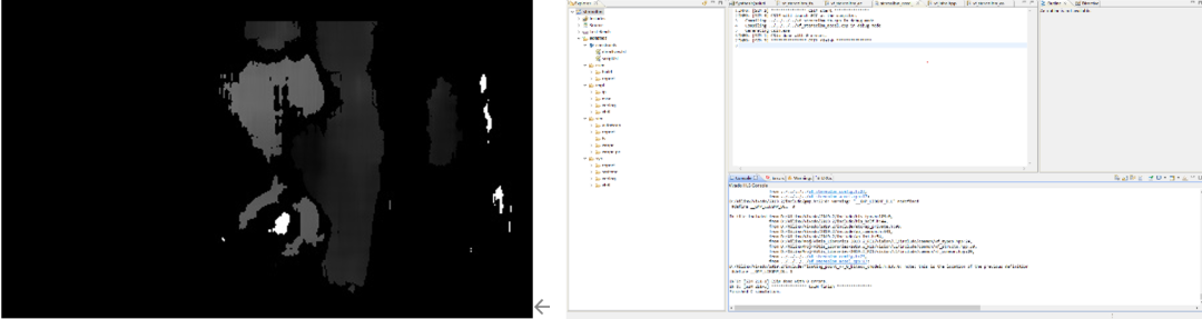
4.2 Acceleration Module Simulation
4.3 CNN QR Code Detection
Compared to natural scenes, the patterns of QR codes have simpler structures and textures. This design constructs a simple **CNN network** targeting this characteristic of QR code images, which includes three convolutional layers, three pooling layers, and two fully connected layers.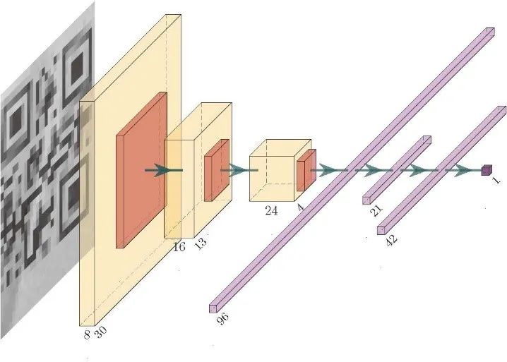 The input image generates different feature maps through different convolution kernels to extract various feature values of the target. Through convolution operations, dimensionality reduction and feature extraction of the input image can be accomplished. To further reduce the dimensionality of the feature map and decrease FPGA resource consumption, a pooling layer is added after each convolution layer to reduce the spatial size of the data and control overfitting. The fully connected layer is a matrix multiplication, equivalent to a feature space transformation, which can extract and integrate useful information. The main goal of the fully connected layer is dimensional transformation, turning high-dimensional data into low-dimensional data. After the above operations, the probability of the input image containing a QR code can be obtained.
4.4 Overall Test Results of Modules and Systems
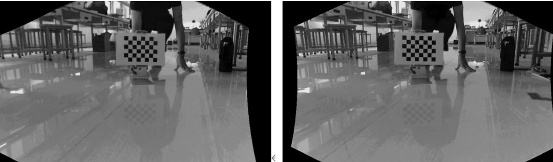
Two cardboard boxes were placed outdoors as path obstacles for overall system testing. The following image is extracted from the video showing the vehicle performing obstacle avoidance operations on the second obstacle. From the positions of the two obstacles in the reference image, it can be seen that when the front object is too close during forward movement, an obstacle avoidance operation is performed. When the obstacle is no longer directly in front of the vehicle, it continues to move forward, achieving the effect of obstacle avoidance.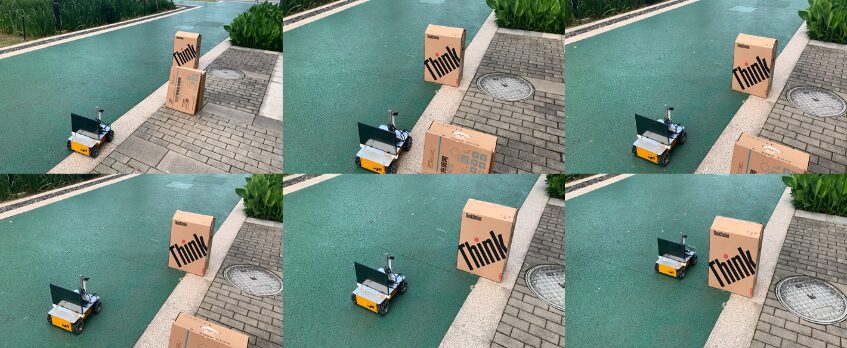
5. Competition Experience
Through this competition, we gained a preliminary understanding of SOC design based on ARM cores. The combination of ARM core and co-processor allows the entire system to outperform common embedded systems and average performance PCs in terms of image acquisition performance, power consumption, and cost when calculating depth images. Compared to traditional microcontrollers that serially collect camera data and transmit single pixels for display, the stable disparity map calculations that are difficult to achieve on PCs are implemented by hardware in this system, greatly reducing the CPU load. The FPGA chip used in this design is the **Xilinx FPGA Artix XC7A200T**. During the competition, we found that when the LUT consumption exceeds 10W and usage exceeds 70%, the wiring time will increase exponentially, and timing will be difficult to converge.
Recommended Reading


【2021 Innovation Competition Work Sharing】 Issue 4 | Gesture Recognition Scheme for Smart Ward Based on ARM Core


【2021 Innovation Competition Work Sharing】 Issue 3 | Cortex-M3 Voice Recognition Sound Source Localization System


【2021 Innovation Competition Work Sharing】 Issue 2 | Real-Time Face Mask Detection SoC Based on ARM Cortex-M3 Processor and Deep Learning Accelerator
END


About Anxin Education


Anxin Education is an innovative education platform focusing on AIoT (Artificial Intelligence + Internet of Things), providing a comprehensive AIoT education solution from primary and secondary schools to higher education.
Anxin Education relies on Arm technology to develop ASC (Arm Smart Interconnection) courses and talent cultivation systems. It has been widely applied in university-industry research cooperation and K-12 STEM education, aiming to cultivate talents in the intelligent interconnection field that meet the demands of the times.