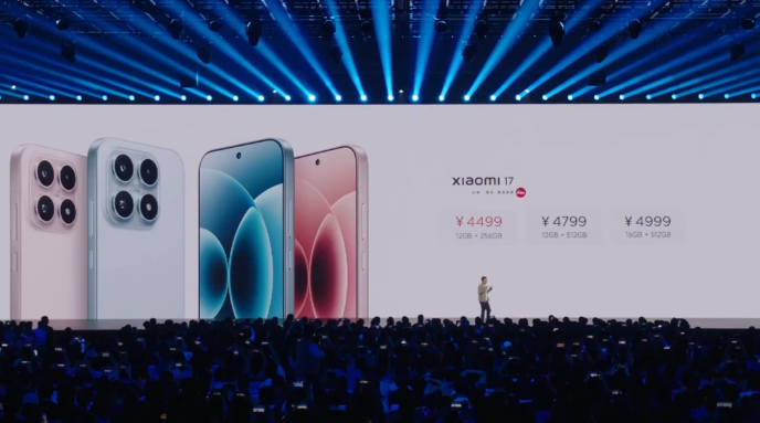
On September 25, Xiaomi founder Lei Jun delivered his sixth annual speech. The highlight was the launch of the new Xiaomi 17 series smartphone. The Xiaomi 17 features the world’s first fifth-generation Snapdragon 8 Supreme Edition, manufactured using TSMC’s third-generation 3nm process technology, with a CPU frequency reaching 4.6GHz, showcasing outstanding performance.
Lei Jun stated that chips are the essential path to Xiaomi’s success, emphasizing that self-developed mobile SoCs must be pursued for at least ten years with an investment of at least 50 billion yuan.
Today, we will focus on analyzing the mobile chip industry.
 Data Chart: Research Database
Overview of the Mobile Chip Industry
Types of Mobile Chips
Every generation of smartphone innovation and iteration is accompanied by upgrades and breakthroughs in the chips behind them. Smartphone chips carry numerous functions, including communication, computation, and storage, and can be categorized into processing chips, baseband chips, RF chips, storage chips, analog chips, and sensor chips.
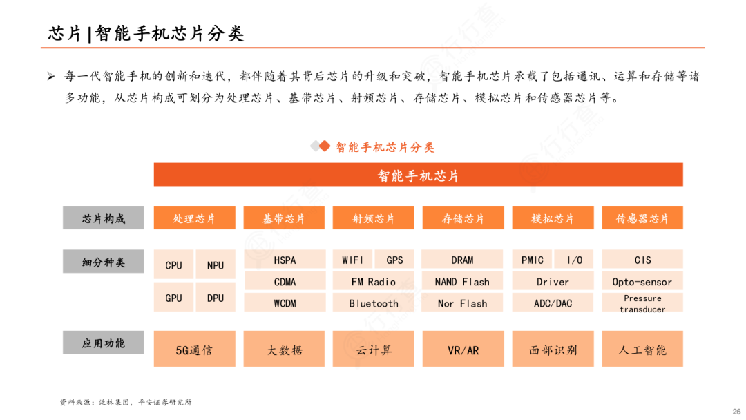
1) Processing Chips
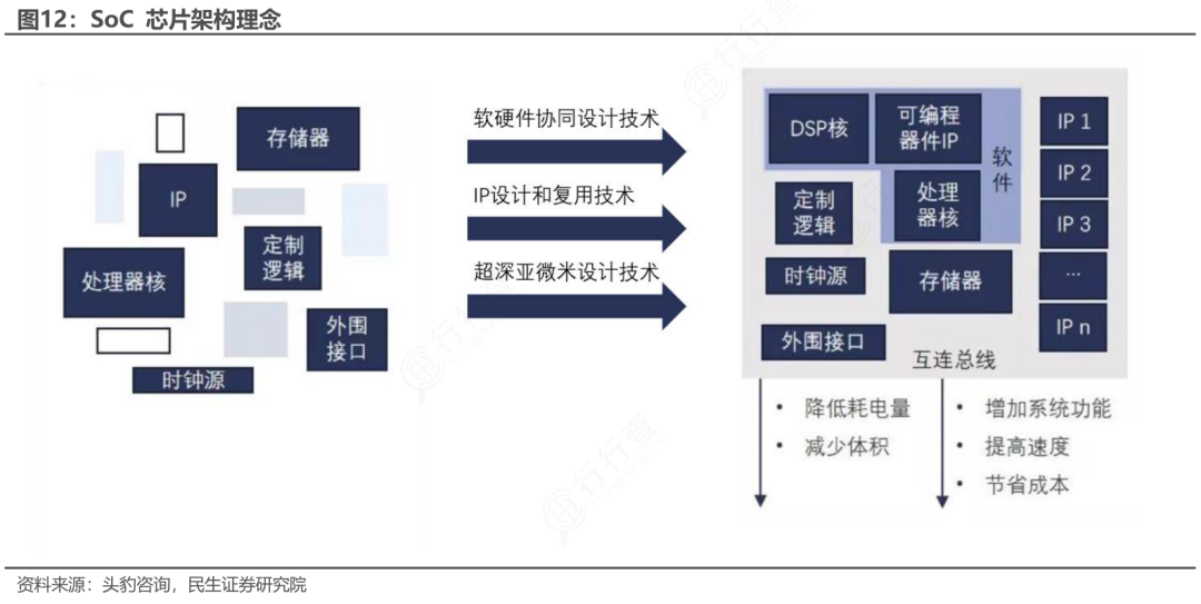
Also known as system-on-chip (SoC), these are the “core hub” of the smartphone, integrating multiple functional modules. Centered around the CPU (central processing unit), it is responsible for executing calculations, task scheduling, and ensuring that multiple applications run simultaneously; it also integrates a GPU (graphics processing unit) for image rendering and game graphics generation; and includes an NPU (neural processing unit) specifically for AI computations, such as facial recognition and real-time responses from voice assistants. Additionally, processing chips may integrate modules like ISP (image signal processor) to coordinate the work of other chips, making it a core determinant of smartphone performance.
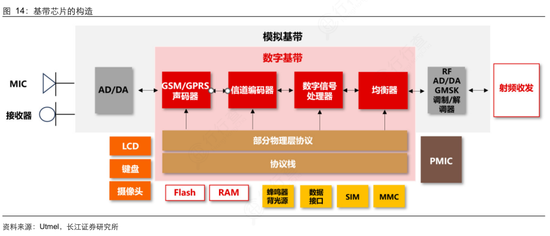
2) Baseband Chips
These are fundamental for enabling voice calls and internet connectivity on smartphones, modulating internal digital data into signals that can be transmitted over wireless networks, or demodulating received wireless signals back into digital data, facilitating communication between the smartphone and base stations. Baseband chips support different generations of mobile communication while ensuring call clarity, network connection stability, and data transmission rates.
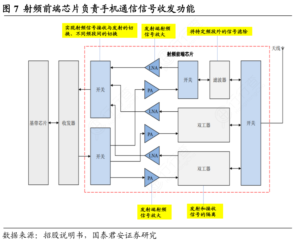
3) RF Chips
These handle high-frequency wireless signals, performing tasks such as signal reception, amplification, and filtering. On the receiving end, they amplify weak high-frequency signals sent from the base station and filter out interference before passing them to the baseband chip; on the sending end, they amplify the processed signals from the baseband chip to an appropriate power level for transmission via the antenna, directly affecting the smartphone’s signal coverage and anti-interference capabilities.
4) Storage Chips
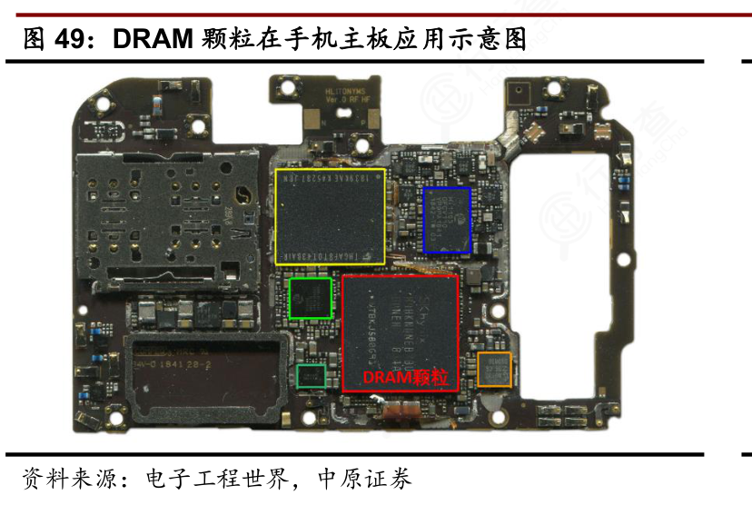
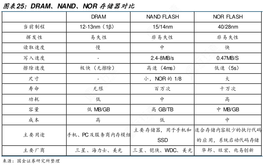
These serve as the data repository for smartphones and are divided into two types: one is DRAM (Dynamic Random Access Memory), used for temporarily storing real-time data during smartphone operation, such as open applications and cached information; data is lost when power is off, and capacity and speed directly affect the smoothness of multitasking on smartphones.
The other type is NAND Flash (flash memory), used for permanent data storage, such as system files, photos, applications, etc.; data is retained even when power is off, determining the smartphone’s storage capacity and file read/write speed.
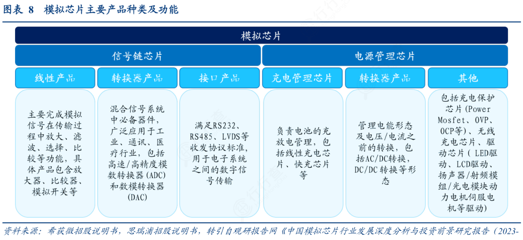
5) Analog Chips
These are responsible for processing the conversion between continuously varying analog signals and discrete digital signals. They include power management modules that allocate stable voltage and current to various components of the smartphone, controlling charging and power consumption; they also include audio processing modules that convert digital audio signals into analog signals to drive speakers or convert analog sound signals received by microphones into digital signals; through ADC (Analog-to-Digital Converter) and DAC (Digital-to-Analog Converter), they adapt sensor signals and external electrical signals to digital circuits, serving as the key link between “real-world signals” and “digital systems” in smartphones.
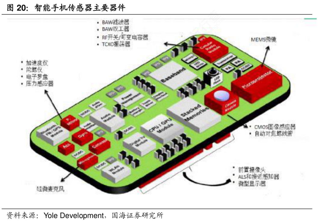
6) Sensor Chips
These are responsible for collecting external environmental information and user operation signals, with common types including:
-
MEMS sensors (Micro-Electro-Mechanical Systems), such as accelerometers and gyroscopes, which perceive the motion state and posture changes of the smartphone, supporting functions like step counting and screen rotation;
-
Image sensors, which capture light and convert it into electrical signals, forming the basis for smartphone photography and video recording;
-
Biometric sensors, such as fingerprint sensors and facial recognition sensors, which achieve identity verification by collecting biological features;
-
Environmental sensors, such as temperature sensors and pressure sensors, which gather data on environmental temperature and altitude, assisting in weather forecasting and location calibration.
The R&D Process of Mobile Chips
The R&D of mobile chips is a typical capital-intensive and technology-intensive process, requiring seven core stages, with a full cycle typically lasting 18-24 months or even longer. The baseband chip development cycle is longer due to the involvement of communication protocol stack development. The overall process is roughly as follows:
1) Front-end Design: Define chip functions based on requirements, complete RTL-level code writing and simulation verification; this stage determines the architecture and performance ceiling of the chip.
2) Back-end Design: Conduct physical layout and routing; as the process shrinks to the 3nm level, layout complexity increases exponentially, requiring advanced technologies like FinFlex architecture to optimize device density.
3) Tape-out: Commission a wafer foundry to produce test samples; the number of photomask layers directly affects the tape-out cycle, with 3nm chips requiring over 100 layers, and tape-out costs reaching tens of millions of dollars.
4) Software Debugging: Integrate protocol stacks and drivers, focusing on identifying software bugs; the debugging cycle for new communication standards can extend by over 50%.
5) Field Testing: Conduct hardware compatibility tests in laboratory and outdoor scenarios; additional local operator network adaptation is required for overseas markets.
6) Operator Certification: Pass operator entry tests, such as Verizon’s PTCRB certification and China Mobile’s CMCC certification.
7) Mass Production Supply: Complete iterative optimization from engineering samples to mass production versions, collaborating with terminal manufacturers for PCBA integration testing.
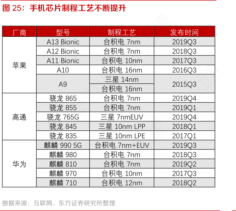
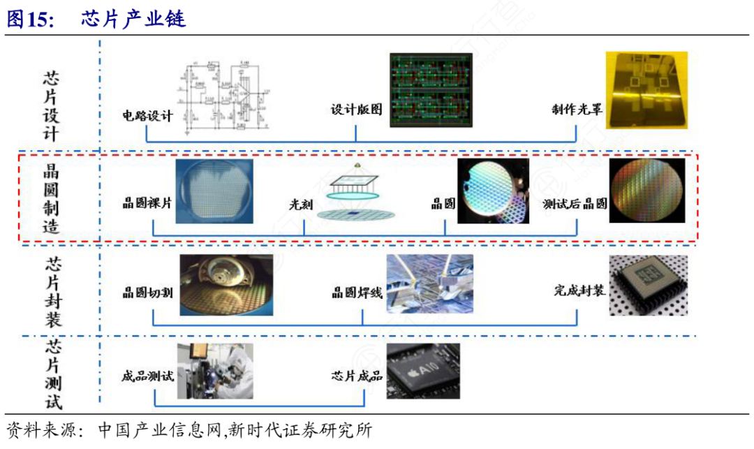
Mobile Chip Manufacturing Processes
The manufacturing process of mobile chips is a core indicator determining performance and power consumption, showing a trend of “decreasing nanometer numbers and increasing integration levels.”
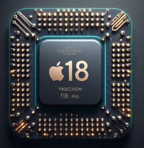
Current mainstream flagship chips have entered the 3nm era, such as Apple’s A18 Pro and Qualcomm’s Snapdragon 8 Elite, both utilizing TSMC’s 3nm process. The 2nm process has entered trial production stages, further optimizing current control through architectural upgrades. However, as the process approaches physical limits, costs increase exponentially, and issues like quantum tunneling effects are becoming more pronounced, diminishing the marginal benefits of process iteration.
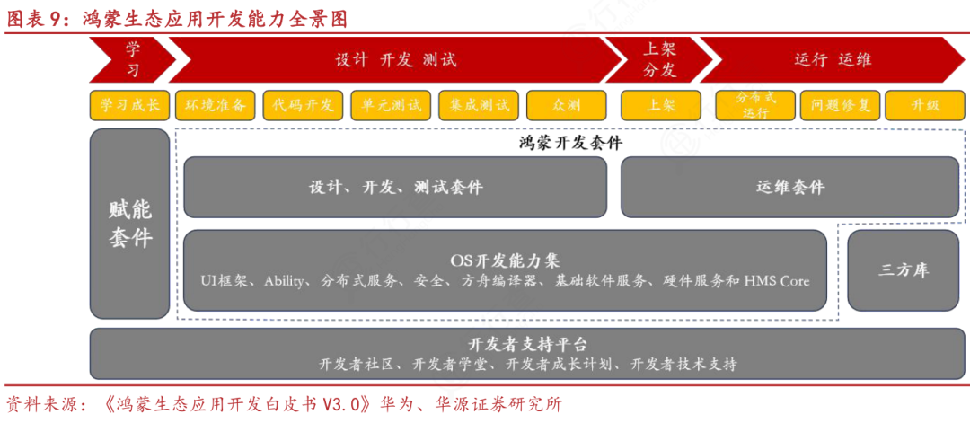
Mobile Chips and the Ecological Collaboration with Operating Systems and Applications
The ecological collaboration between mobile chips and various software is key to unleashing chip performance. Chips open hardware features to the system through standardized interfaces, such as AI computing power and graphics rendering capabilities, providing foundational support for the application layer; the operating system builds a resource scheduling framework, dynamically allocating chip computing power, storage, and other resources, balancing performance and power consumption, while allowing various applications to conveniently call hardware functions through API interfaces. Application software optimizes based on chip and system characteristics, unleashing hardware capabilities for various specific applications.
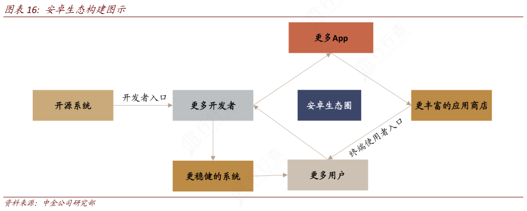
Apple achieves deep optimization through a closed ecosystem, with the A-series chips’ self-developed instruction set highly compatible with the iOS compilation chain. The Android camp builds compatibility advantages through an open ecosystem, achieving dynamic optimization of application code; Huawei’s HarmonyOS ecosystem focuses on “distributed technology,” with Kirin chips integrating NPU, ISP, and other dedicated modules, deeply adapting to HarmonyOS’s distributed architecture, enabling seamless collaboration between chips and multiple terminals.
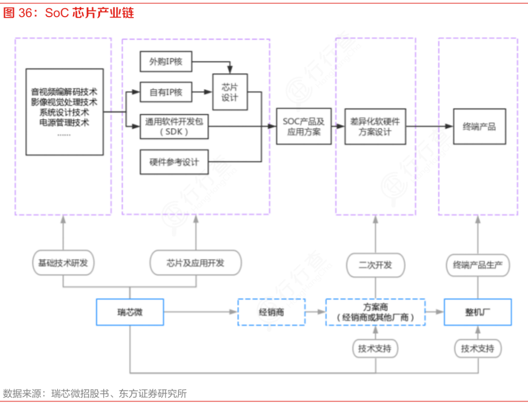
The Mobile Chip Industry Chain
The upstream of the mobile chip industry chain focuses on raw materials and core equipment.
Silicon wafers are the foundation of mobile chips, provided by domestic companies such as Zhonghuan Co. and Hu Silicon Industry. Key materials like photoresists, sputtering targets, and electronic special gases rely on manufacturers like Yongda Photoelectric and Jiangfeng Electronics, although some high-end products still need to be imported. In the equipment sector, photolithography machines are the “bottleneck” core, with ASML monopolizing the EUV photolithography market. Shanghai Microelectronics’ 28nm equipment is expected to enter mass production in the coming years, while Zhongwei’s 5nm etching machine has been certified by TSMC, and North Huachuang’s thin-film deposition equipment has entered the SMIC production line. Additionally, EDA tools and IP cores are also critical upstream components supporting chip design.
The midstream is a technology-intensive area, including design, manufacturing, and packaging testing. In the chip design phase, Qualcomm and MediaTek dominate the mid-to-high-end market, while Apple’s A-series chips stand out due to their iOS ecosystem advantages, and Huawei’s HiSilicon Kirin chips have achieved breakthroughs in the domestic high-end market. On the manufacturing side, TSMC holds over 70% of the global advanced process share, with 3nm technology already in mass production; SMIC has achieved trial production of 5nm, with a 14nm yield reaching industry levels. In the packaging and testing sector, Changdian Technology ranks among the top globally, mastering 3nm Chiplet packaging technology, with HBM packaging capabilities comparable to Samsung.
The downstream applications are extensive, with smartphones remaining the largest market, driving demand for flagship chips like Qualcomm’s Snapdragon and MediaTek’s Dimensity. With the development of AI and the Internet of Things, chips are extending into automotive-grade and industrial control fields. 5G/6G communication is driving upgrades in RF chips, with Huawei and Qualcomm’s baseband chips leading the technological frontier.
Market Size of Mobile Chips
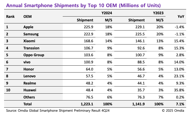
According to market research firm Omdia, the total shipment of smartphones in 2024 is expected to reach 1.223 billion units, a 7.1% increase from 1.142 billion units in 2023, indicating a steady recovery in the industry.
(Data as of February 2025)
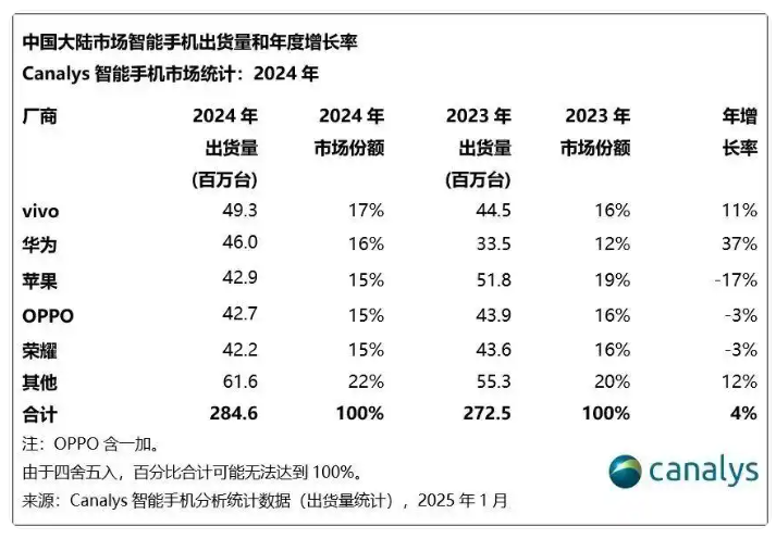
According to Canalys, the shipment of smartphones in mainland China is expected to reach 285 million units in 2024, a year-on-year increase of 4%. Canalys predicts that the shipment of smartphones in the Chinese market will exceed 290 million units in 2025.
(Data as of January 2025)
According to Qunzhi Consulting, the global shipment of smartphone chips is expected to be approximately 1.21 billion units in 2024, a year-on-year increase of 5.8%.
Chip brands like Qualcomm and MediaTek continue to dominate the market, with Qunzhi Consulting estimating that the global shipment of Qualcomm and MediaTek smartphone APs will be around 740 million units in 2024, achieving a combined market share of 61.5%. Domestic brands like HiSilicon and Unisoc are also making strides, with domestic brand chip market share reaching 12.8%.
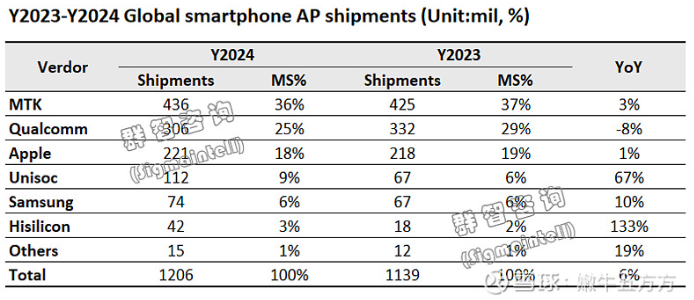
(Data as of January 2025)
According to Business Research Insights, the global 4G smart device chip market is expected to maintain continuous growth from 2023 to 2032. The market size for 4G baseband chips is expected to exceed $3.5 billion in 2024, reaching $8.515 billion by 2032.
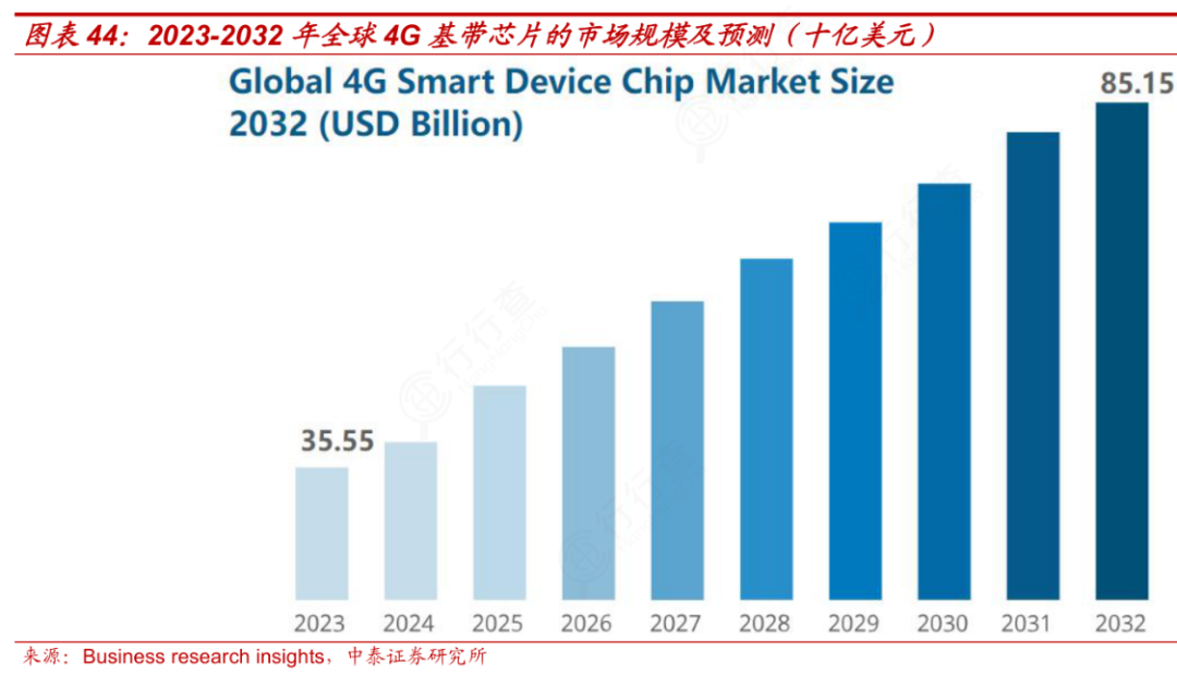
(Data as of April 2025)
The global 5G baseband chip market size is expected to reach $2.27 billion in 2024, with annual growth projected to approximately $59.98 billion by 2032.
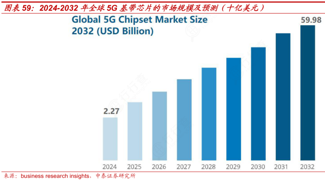
(Data as of April 2025)
Technical Routes of Mainstream Chip Manufacturers
1) Qualcomm: Focused on a “full-stack technology layout,” it holds an absolute advantage in the baseband chip field, with the Snapdragon X series baseband consistently leading in 5G speed and multi-mode compatibility. By acquiring Nuvia, it has developed its own Oryon architecture CPU, reducing reliance on ARM’s public version. Its strategic focus is on building a “chip + software + ecosystem” full-chain competitiveness, deeply binding with flagship Android models.
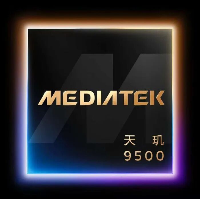
2) MediaTek: Following a “cost-performance breakthrough + high-end attack” route, it occupies a large share in the mid-to-low-end market with the Dimensity 700/800 series, while achieving performance parity with Qualcomm in the high-end market through the Dimensity 9000/9500 series. It has also added customized modules for imaging ISP and AI processing, attracting flagship models from brands like Xiaomi and Vivo, breaking Qualcomm’s monopoly with a strategy of “balanced performance + cost control.”
3) Apple: Focused on “self-developed architecture + software-hardware collaboration,” the A-series chips use self-developed CPU/GPU architecture, not relying on ARM’s public design. For example, the A18 Pro’s 6-core CPU includes 2 performance cores and 4 efficiency cores, achieving extreme matching of chip performance and system smoothness through deep optimization of iOS’s task scheduling mechanism.
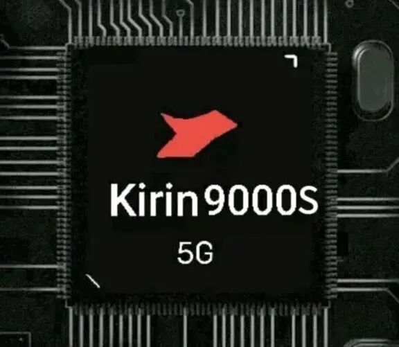
4) Huawei: Huawei HiSilicon focuses on “domestic substitution + HarmonyOS ecological collaboration.” Due to external restrictions, it is currently prioritizing the adaptation of chip design to domestic manufacturing processes, while leveraging Kirin chips and HarmonyOS’s distributed technology to achieve computing power sharing and resource scheduling across multiple devices. The core of its technical route is to build a self-controllable chip ecosystem.
(Public data compilation, industry research sharing, not for investment advice)
(END)
– Author Introduction –
Contact: jaydata888


Jay’s Industry Universe
Author of “Illustrated 100 Industry Chains”
Author of “Illustrated 100 Business Models”
–  Book Gift Package
  –(Gift 1: 2025 Industry Analysis Framework Video Course)(Gift 2: Hundreds of PDF Industry Book Drafts)(Gift 3: AI Toolkit for Industry Research 7-day VIP)