
Click the blue text to follow us

Chip development generally includesfour stages: chip design, production of samples, testing and validation, and mass production. After completing the chip design, engineers need to obtain some chip samples to test and validate whether the newly developed chip meets the design requirements in terms of functionality and performance. If the samples pass the tests, mass production and commercialization can proceed as planned; if the samples have design flaws, the chip design needs to be modified, and new samples must be produced for testing.

Chip Development Process
Full Mask and MPW are two different chip fabrication methods used in the chip development process.
Full Mask means using a full set of masks, where all the masks are specifically used for producing the same chip.This fabrication method is very expensive, with costs around $5 million for a 14nm process and about $15 million for a 7nm process, including the masks and one run of fabrication. Such high production costs are unaffordable for small and medium-sized chip development companies, universities, and research institutions.Only when there is complete confidence in the design’s success and readiness for mass production will the Full Mask method be chosen.
Therefore, during the sample production phase, chip design companies can use MPW to complete sample production in the most cost-effective way.MPW stands for Multi-Project Wafer, which allows multiple chip design projects with the same manufacturing process to be produced on the same wafer.After production, each chip design project can obtain dozens to hundreds of chip samples, which R&D engineers use to test and validate the correctness of the chip design. The MPW fabrication costs are shared among all participating companies based on the chip area, resulting in very low fabrication costs.

Samsung’s 2025 MPW Schedule
MPW is usually organized by foundries or third-party service providers,with the MPW time points for each process predetermined throughout the year, referred to as Shuttle, which departs at scheduled times, so participants often refer to joining an MPW as catching a certain shuttle. This creates significant pressure on the design and development of chips, and when foundry capacity is tight, MPW sessions may be canceled, leading to delays in product launches.
MPW Fabrication Services
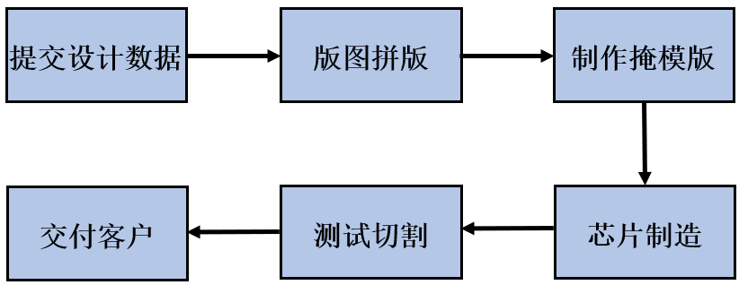
MPW Process
-
Submit Design Data: After confirming participation in a specific MPW, customers must submit layout files, netlists, test vectors, and other data before the deadline.
-
Layout Assembly: The foundry or third-party service provider will perform DRC and LVS checks, then arrange and combine the layouts of these projects according to certain rules to generate unified layout data.
-
Mask Production: The foundry will produce masks based on the assembled layouts.
-
Chip Manufacturing: The foundry will manufacture chips for multiple projects simultaneously according to the specified process flow.
-
Testing and Dicing: The completed wafers undergo WAT and CP testing, followed by dicing to separate chips from different projects. Customers can choose third-party service providers for packaging and testing services or can commission other institutions themselves.
-
Delivery to Customers: The tested and qualified chips are delivered to customers, who then perform functional validation and optimize the design based on the structure.
MPW and Full Mask complement each other, covering the entire R&D process from chip design to mass production. Without MPW fabrication services, many small and medium-sized chip design companies would be unable to conduct chip design and development, thusthe important role of MPW is to significantly reduce chip R&D costs. When chips enter mass production,Full Mask fabrication can reduce long-term production costs, accelerate commercialization, and ensure mass production performance, all of which directly determine the market competitiveness of the product.
Thank you for reading my article. If you found it helpful, please give me afollow. Let’s continue our discussion next time.
>/ Author: Xiao Xin Ji