In modern SoC (System-on-Chip) design, the CRG (Clock and Reset Generator) serves as the “heart” and “nervous system” of the entire chip, responsible for providing stable, reliable, and controllable clock and reset signals for the system. The quality of the CRG module’s design directly affects the chip’s functional correctness, power consumption performance, testability, and overall timing performance. This article systematically introduces the two core components of the CRG module: Clock System and Reset System, covering their basic structure, key circuit modules, and design points.
1. CRG Clock System
The main function of the clock subsystem in the CRG is to generate various clock signals with different frequencies, phases, duty cycles, and timing characteristics from an external low-frequency reference clock to meet the needs of different functional modules. Typical clock paths include the following key modules:
1. Clock Source
The clock source usually comes from an external crystal oscillator, commonly found as:
- 32.768 kHz: Used for real-time clock (RTC) modules, supporting low-power timing and wake-up functions;
- 24 MHz or 26 MHz: Used as the reference input clock for the main PLL, widely applied in communication and high-performance processor systems.
These external crystal oscillators are driven by on-chip oscillation circuits and enter the CRG module for subsequent processing.
2. Phase-Locked Loop (PLL)
PLL is the core module of the clock system, which functions to “multiply” the low-frequency reference clock to a high-frequency, low-jitter, and high-stability system main clock (such as 1 GHz, 2 GHz, etc.). The PLL achieves frequency locking through a feedback control mechanism, outputting clock signals with precise frequency and phase relationships.
A typical PLL structure includes:
- Phase Frequency Detector (PFD)
- Charge Pump (CP)
- Loop Filter (LF)
- Voltage-Controlled Oscillator (VCO)
- Feedback Divider
The clock output from the PLL is typically used for high-performance modules such as CPU, GPU, and DDR controllers.
3. Clock Divider
To meet the frequency requirements of different modules (such as peripheral interfaces usually operating at lower frequencies), the CRG uses dividers to perform integer or fractional division of the high-frequency clock output from the PLL, generating clock signals such as 100 MHz, 50 MHz, 25 MHz, etc.
The divider can be fixed or programmable, allowing software to dynamically adjust system performance and power consumption.
4. On-Chip Clock Controller (OCC)
The OCC is mainly used for chip testing in DFT (Design for Test) scenarios. In ATE (Automatic Test Equipment) testing, it is necessary to switch the internal clock of the chip to the test clock provided by the external test machine (ATE Clock) for full-speed functional verification.
The OCC typically includes a Clock Multiplexer (Mux), controlled by test mode signals (such as scan_mode), to switch between the internal clock and the ATE clock.
5. Integrated Clock Gating (ICG)
ICG is a key technology for reducing dynamic power consumption. It controls whether to pass the clock to downstream logic modules through an enable signal. When a module is not in operation, turning off the clock can significantly reduce unnecessary switching power.
ICG is generally integrated into the standard cell library and comes in two common forms:
- Register-Level ICG: Automatically inserted by synthesis tools;
- Module-Level ICG: Manually added by designers to control the clock switch of the entire subsystem.
⚠️ Note: ICG must be synchronized with the enable signal to avoid glitches.
6. Clock Switching
The system often needs to dynamically switch between multiple clock sources (e.g., switching from PLL to a low-frequency clock to enter sleep mode). Depending on whether “dynamic switching” is allowed, it can be divided into two categories:
(1) Ordinary Clock Multiplexer
- Belongs to combinational logic circuits;
- Only suitable for static switching (i.e., both clocks are off during switching);
- If switching occurs while the clock is running, it is easy to produce glitches, leading to logical errors.
assign clk_out = (sel == 1'b0) ? clk0 : clk1;(2) Glitch-Free Clock Switching Circuit
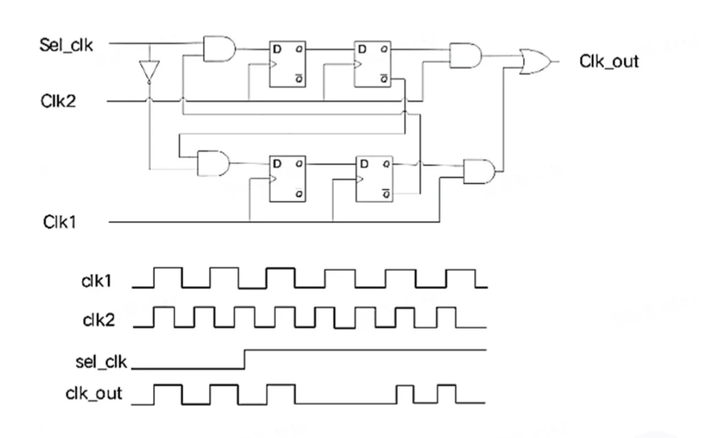
Used for dynamic switching, ensuring no glitches occur during the switching process. A typical structure is as follows:
- Samples the selection signal using the falling edges of both clocks;
- Ensures that only one clock is valid at any time through a feedback mechanism;
- Finally merges the output through an “OR gate” to achieve smooth switching.
✅ Design Principle: Complete the switch when both clocks are low, effectively avoiding glitches.
This circuit is widely used in clock switching scenarios under power management modes.
7. Clock Buffer / Clock Tree
Due to the large load driven by clock signals and their wide distribution, a dedicated Clock Tree is required for fan-out and delay balancing. The clock buffer in the CRG is used to enhance driving capability, reduce skew, and insertion delay, ensuring that clock signals maintain good integrity throughout the chip.
2. CRG Reset System
The role of the reset system is to force all registers and state machines of the chip to a known initial state during power-up or abnormal conditions, ensuring that the system can reliably start or resume normal operation.
1. Reset Source Classification
Reset signals can come from outside or inside the chip:

The reset signal of a module is often the result of multiple reset sources combined through “OR” logic, ensuring that any exception can trigger a reset.
2. Reset Types and Their Characteristics
Based on the relationship between reset and clock, reset methods can be mainly divided into three types: synchronous reset, asynchronous reset, and asynchronous reset with synchronous release.
2.1 Synchronous Reset
The reset signal is effective only on the valid edge of the clock (usually the rising edge).
Verilog Example:
always @(posedge clk) begin
if (!rst_n) begin
        q <= 1'b0;
end else begin
        q <= d;
end
end
Advantages:
- Fully synchronous, beneficial for static timing analysis (STA);
- Can naturally filter glitches in the reset signal (requires clock presence);
- Results in a clean circuit after synthesis, suitable for high-frequency path design.
Disadvantages:
- The reset pulse must last at least one clock cycle; otherwise, it may not be captured;
- If the clock is gated or not stable, the reset is ineffective;
- Most standard cell libraries do not support synchronous reset DFFs, requiring additional combinational logic implementation, increasing data path load.
📌 Applicable Scenarios: Internal condition resets, modules with strict timing requirements.
2.2 Asynchronous Reset
As long as the reset signal is valid (e.g., low level), it immediately resets the register regardless of the clock state.
Verilog Example:
always @(posedge clk or negedge rst_n) begin
if (!rst_n) begin
        q <= 1'b0;
end else begin
        q <= d;
end
end
Advantages:
- Can reset immediately upon power-up without waiting for the clock;
- Independent of the clock, suitable for gated clock or standby wake-up scenarios;
- Widely supported by standard cell libraries, with low resource overhead.
Disadvantages:
- If the reset release does not meet the recovery/hold time, it may cause metastability;
- High quality requirements for the reset signal, susceptible to noise and glitches;
- Reset release is not synchronized, which may cause some modules to exit reset first, leading to inconsistent states.
📌 Applicable Scenarios: Global reset, power management, low-power mode switching.
2.3 Asynchronous Reset with Synchronous Release
This is the most recommended reset strategy in the industry, combining the immediacy of asynchronous reset with the safety of synchronous release.
Core Idea:
- When the reset arrives: Immediately asynchronously reset all registers;
- When the reset is released: Synchronize the reset signal to the target clock domain through two levels of synchronous flip-flops to avoid metastability propagation.
Verilog Implementation:
reg rst_sync1, rst_sync2;
always @(posedge clk or negedge arst_n) begin
if (!arst_n) begin
        rst_sync1 <= 1'b0;
        rst_sync2 <= 1'b0;
end else begin
        rst_sync1 <= 1'b1;
        rst_sync2 <= rst_sync1;
end
end
assign core_rst_n = rst_sync2;
Working Process:
- When
<span>arst_n</span>is pulled low, both registers are immediately cleared, and the system enters reset; - When
<span>arst_n</span>is pulled high, the first register is set to 1 at the next clock rising edge, and the second register is delayed by one cycle; - Finally,
<span>core_rst_n</span>is released after two clock cycles, completing the “synchronous release”.
✅ Advantages: Ensures timely power-up reset while avoiding metastability risks during reset release.
3. Summary and Recommendations

💡 Design Tips: “A good CRG design is the foundation for functional correctness, low power consumption, easy testing, and high reliability.” A clear CRG architecture should be defined early in SoC development and integrated throughout the RTL design, synthesis, STA, and DFT processes.
References
- Analysis of Clock Mechanisms in CRG Design – CSDN Blog
- The Art of Hardware Architecture: Design Methods and Techniques for Digital Circuits
- IC Basics | Reset Section: In-Depth Analysis of Synchronous and Asynchronous Resets – CSDN Blog
- Synopsys Design Compiler User Guide: Clock Gating & Reset Synchronization