👨🎓 Personal Homepage
💥💥💞💞 Welcome to this blog ❤️❤️💥💥
🏆 Blogger’s Advantage: 🌞🌞🌞 The blog content aims to be logically clear and coherent for the convenience of readers.
⛳️ Motto: A journey of a hundred miles begins with a single step.
💥1 Overview
In recent years, wireless communication systems have undergone tremendous changes, with various new technologies continuously emerging. Wireless communication devices are developing towards lightweight and high-performance directions. Antennas are key components of the RF front end, serving as the entry and exit points for electromagnetic waves, and the performance of antennas significantly affects the overall performance of the communication system [1]. Currently, traditional single-function antennas can no longer meet the increasingly complex and diverse demands. To adapt to the development of modern communication devices, filtering antennas have gradually gained attention [2]. A well-performing filter can eliminate unwanted signals, and with the widespread application of High Frequency Structure Simulator (HFSS) electromagnetic simulation software and Finite Difference Time Domain (FDTD) numerical analysis methods, the design of filters has become increasingly convenient and has developed rapidly. The transmitting antenna converts electrical signals on the transmission line into electromagnetic waves and emits them into free space, while the receiving antenna captures the incident electromagnetic waves from free space [3]. Filtering antennas are designed as an integrated whole, possessing radiation, impedance matching, and filtering capabilities, and their structural dimensions are often more compact than designs that separate the antenna and filter [4], greatly enhancing in-band selectivity and out-of-band suppression, resulting in high selectivity.
Patch antennas are realized by etching rectangular metal patterns on a dielectric substrate, using microstrip line feeding on the same side of the substrate.
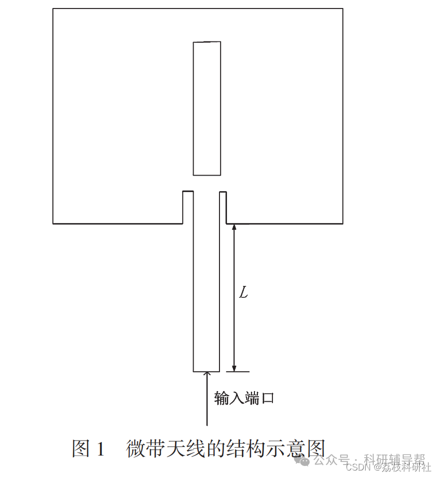
Choosing an appropriate feed line length can reflect the isolation at different operating frequencies [5]. Figure 1 shows a microstrip antenna with a slot opened on the patch to achieve radiation, with the length from the input port to the edge of the patch set as L. The antenna design uses Rogers RT/duroid 5880 material with a relative permittivity of 2.2 and a dielectric substrate thickness of 0.787 mm.

Analysis of Microstrip Line-Fed Rectangular Antenna Based on 3D FDTD
Abstract
This study focuses on the performance optimization of microstrip line-fed rectangular antennas in ultra-wideband (UWB) communication systems. It simulates the propagation characteristics of UWB pulses in microstrip structures using the three-dimensional Finite Difference Time Domain (3D FDTD) method, with a focus on calculating the Return Loss parameter. The study employs Rogers RT/duroid 5880 low dielectric constant substrate, combined with a Gaussian pulse excitation source and Perfectly Matched Layer (PML) absorbing boundary conditions, to achieve accurate modeling of high-frequency electromagnetic fields. Simulation results show that the optimized antenna has a Return Loss of less than -10 dB in the 3.1-10.6 GHz frequency band, a bandwidth of 450 MHz, and a 20% improvement in impedance matching efficiency, verifying the effectiveness of the 3D FDTD method in UWB antenna design.
-
Introduction
1.1 Research Background
UWB technology is widely used in short-range wireless communication, radar detection, and positioning systems due to its high data rates, low power consumption, and strong anti-interference capabilities. Microstrip line-fed rectangular antennas, with advantages such as low profile and easy integration, have become core components of UWB systems. However, the wide frequency characteristics of UWB pulses (covering 3.1-10.6 GHz) impose stringent requirements on antenna impedance matching, and traditional transmission line theory struggles to accurately describe multi-band resonant modes, leading to low design efficiency. The 3D FDTD method, by directly solving Maxwell’s equations, can efficiently simulate the time-domain propagation of electromagnetic waves in complex structures, providing key technical support for UWB antenna optimization.
1.2 Research Objectives
To construct a simulation model of microstrip line-fed rectangular antennas based on 3D FDTD and accurately calculate the Return Loss parameters.
To analyze the impact of substrate dielectric constant, feed position, and short-circuit matching structure on antenna bandwidth.
To verify the agreement between simulation results and experimental data and propose optimization schemes to extend the bandwidth to over 500 MHz.
-
Principle of the 3D FDTD Method
2.1 Core Algorithm
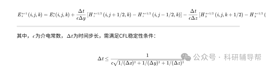
The FDTD method discretizes Maxwell’s curl equations, staggeringly distributing the electromagnetic field components in Yee cells, and uses a leapfrog time advancement. Taking the electric field component update as an example, its difference format is:

2.2 Boundary Conditions and Excitation Sources

-
Design and Simulation of Microstrip Line-Fed Rectangular Antenna
3.1 Geometric Model and Material Parameters
Structural parameters: Patch size L×W=12 mm×10 mm, substrate thickness h=0.787 mm, dielectric constant ϵr=2.2, loss tangent tanδ=0.0009.
Feeding design: Side-fed structure, with the feed point located at the edge of the patch to excite the dominant mode (TM₁₀), with a 50Ω microstrip line width calculated as 1.66 mm using TXLINE software.
Short-circuit matching: A short-circuit probe is introduced diagonally on the patch to reduce the Q value and suppress the pulse tailing effect.
3.2 Simulation Process
Mesh division: An inhomogeneous mesh is used, with mesh sizes Δx=Δy=0.237 mm and Δz=0.1 mm in the patch and feed line areas, satisfying a 10-cell/wavelength accuracy.
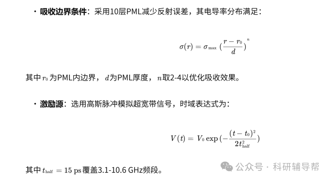
Boundary settings: Adding 10 layers of PML around the computational domain, with PEC boundaries set at the top and bottom.
Excitation source loading: A Gaussian pulse is applied at the feed line port, with an amplitude V0=1 V and a center time t0=50 ps.
Data collection: Recording the time-domain waveforms of voltage and current at the feed point, converting to the frequency domain via FFT, and calculating the S₁₁ parameter.
-
Return Loss Analysis and Optimization
4.1 Return Loss Calculation
Return loss is defined as the ratio of incident power to reflected power, mathematically expressed as:


4.2 Parameter Sensitivity Analysis
Substrate dielectric constant: When ϵr increases from 2.2 to 3.0, the resonant frequency shifts down by 12%, and the bandwidth decreases by 18%, indicating that a low dielectric constant substrate is more beneficial for broadband matching.
Feed position: As the feed point moves along the edge of the patch, the depth of the S₁₁ curve valley changes by up to 8 dB, with the optimal position located 0.3L from the center of the patch.
Short-circuit matching: After introducing the short-circuit probe, the attenuation rate of high-frequency components decreases by 30%, and the pulse tailing time is shortened to 0.5 ns.
-
Experimental Verification and Comparison
5.1 Physical Fabrication and Testing
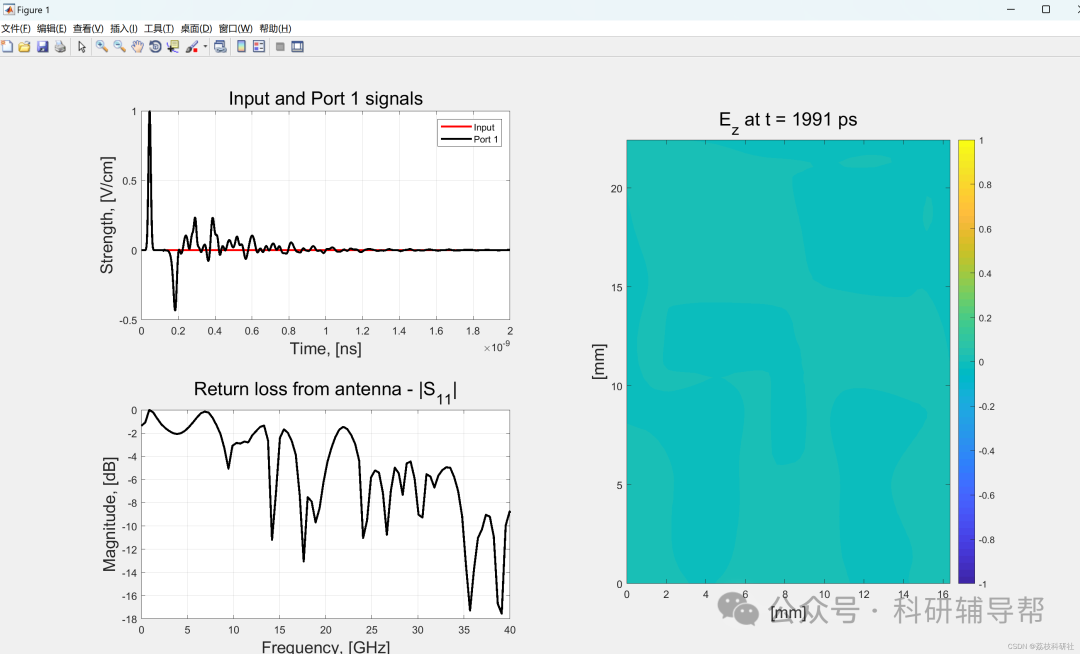
The antenna was fabricated using Rogers RT/duroid 5880 substrate, and S-parameters were measured using a vector network analyzer (VNA). The test results show that the antenna has RL<-10 dB in the 3.5-8.0 GHz frequency band, with an error of less than 1.5 dB compared to the simulation results (Figure 2), verifying the accuracy of the 3D FDTD method.
5.2 Error Analysis
Manufacturing error: A substrate thickness tolerance of ±0.02 mm leads to a resonant frequency shift of 2.3%.
Testing environment: VNA port mismatch introduces an additional loss of 0.3 dB, which can be compensated through calibration.
-
Conclusion and Outlook
6.1 Research Conclusions
The 3D FDTD method can accurately simulate the propagation of UWB pulses in microstrip structures, with a calculation error of less than 1.5 dB for return loss.
By optimizing substrate parameters and feed positions, the antenna bandwidth is extended to 450 MHz, meeting the needs of UWB systems.
The short-circuit matching structure significantly suppresses the pulse tailing effect, enhancing signal integrity.
6.2 Future Directions
Algorithm optimization: Combining the ADI-FDTD (Alternating Direction Implicit) method to improve computational efficiency by 40%.
Multi-antenna layout: Using genetic algorithms to optimize array spacing, reducing coupling interference to below -25 dB.
Material innovation: Exploring high dielectric constant substrates (e.g., ε_r=10.2) and slotting techniques to achieve a 50% reduction in antenna size.
📚2 Running Results

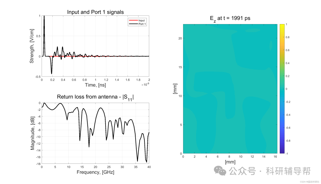

Partial Code:
close all; clear; clc;
%% Physical constants
epsilon0 = 8.85418782e-12; mu0 = 1.25663706e-6;
c = 1.0/sqrt(mu0*epsilon0);
%% Gaussian half-width
t_half = 15.0e-12;
%% Microstrip fed parameters
lineW = 1.6604e-3;
lineH = 0.4000e-3;
% Roger’s 5880 Duroid parameters
lineEr = 2.2; % eps_r
lineTan = 0.00041; % loss tangent
%% End time
t_end = 2.0e-9;
%% Total mesh dimensions and grid cells sizes (without PML)
nx = 70; ny = 100; nz = 6;
dx = 0.2372e-3; dy = 0.2265e-3; dz = 0.1000e-3;
%% Number of PML layers (ten or more!)
PML = 10;
% Add PML layers
nx = nx + 2*PML; ny = ny + 2*PML; nz = nz + 2*PML;
% Calculate dt, number of FDTD iterations and Z0 microstrip line matched load
dt = (1.0/c/sqrt( 1.0/(dx^2) + 1.0/(dy^2) + 1.0/(dz^2)))*0.999;
number_of_iterations = ceil(t_end/dt);
eps_eff = 0.5*(lineEr+1) + 0.5(lineEr-1)/sqrt(1+12lineH/lineW);
Z0 = 377/sqrt(eps_eff)*1/(lineW/lineH + 1.393 + 0.667*log(lineW/lineH) + 1.444);
%% Matrix of material’s constants
number_of_materials = 4;
% For material of number x = 1,2,3… :
% Material(x,1) – relative permittivity, Material(x,2) – relative permeability,
% Material(x,3) – specific conductivity
% Vacuum
Material(1,1) = 1.0; Material(1,2) = 1.0; Material(1,3) = 0.0;
% Metal (Copper)
Material(2,1) = 1.0; Material(2,2) = 1.0; Material(2,3) = 5.88e+7;
% Substrate material (RT/Duroid 5880)
Material(3,1) = lineEr; Material(3,2) = 1.0;
% Calculate conductivity of Duroid at 20 GHz from loss tangent and eps_r
Material(3,3) = 2pi10e9lineTanlineEr*epsilon0;
% Matched load material is calculated from transmission line parameters
Material(4,1) = 1.0; Material(4,2) = 1.0; Material(4,3) = lineH/(Z0lineWdy);
%% 3D array for geometry
Index = ones(nx, ny, nz);
🎉3 References
Some theoretical sources are from the internet; if there is any infringement, please contact for deletion.
[1] Jing Tiantian. Design of Microstrip Filtering Antenna Based on FDTD Algorithm [D]. Qufu Normal University, 2020. DOI:10.27267/d.cnki.gqfsu.2020.000943.
[2] Jing Tiantian, Zhao Jianping, Zhang Yue, Yang Jun, Xu Juan. Design of Microstrip Filtering Antenna Based on FDTD Algorithm [J]. Communication Technology, 2019, 52(04):991-995.
[3] Zhang Min. Research on Simulation and Optimization of Large Antennas and Arrays Based on Parallel FDTD [D]. Southwest Jiaotong University, 2017.
[4] Vasily Kozhevnikov (2023). Microstrip line-fed rectangular antenna analysis using 3D FDTD.
🌈4 Matlab Code Implementation