1. SPI Communication Protocol: The High-Speed Dialogue of Electronic Devices
SPI (Serial Peripheral Interface) is a commonly used synchronous serial communication protocol between electronic devices. Due to its high speed and full-duplex characteristics, it is widely used for communication with peripherals such as memory and sensors.
1.1 Basic Principles (Four-Wire Interaction)
- SCK: Clock signal line (controlled by the master device)
- MOSI: Master Out Slave In
- MISO: Master In Slave Out
- CS: Chip Select signal (active low)
1.2 Communication Features
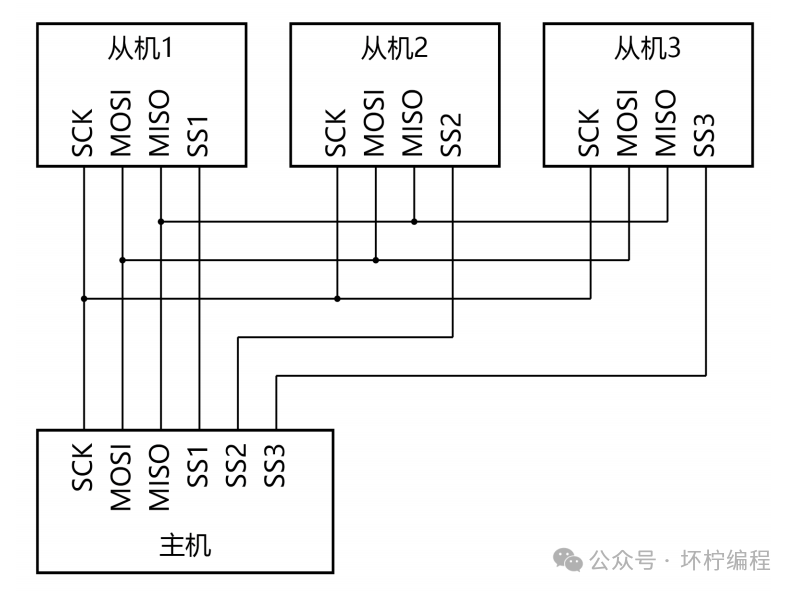
- Master-Slave Mode: One master can control multiple slaves
- Clock Synchronization: Data transfer rate is determined by the master
- Duplex Transmission: Data can be sent and received simultaneously
- Mode Configuration: Four working modes are formed by combining CPOL (Clock Polarity) and CPHA (Clock Phase)
1.3 Working Principle
Simple Principle Breakdown:
- Role Division
- Master (e.g., STM32): Controls the overall process, generates the clock signal (SCK), and controls the data transfer rhythm
- Slave (e.g., W25Q128): Passively responds, participating in communication only when selected by the master
- Data Transfer Process (Example: Sending 0xA3)
- Step 1: The master pulls the corresponding slave’s CS pin low (calling the slave)
- Step 2: The master outputs the clock signal via SCK (setting the communication speed)
- Step 3: The master sends data bit by bit via MOSI (0b10100011)
- Step 4: The slave simultaneously returns data via MISO (full-duplex feature)
- Step 5: The master pulls CS high to end communication
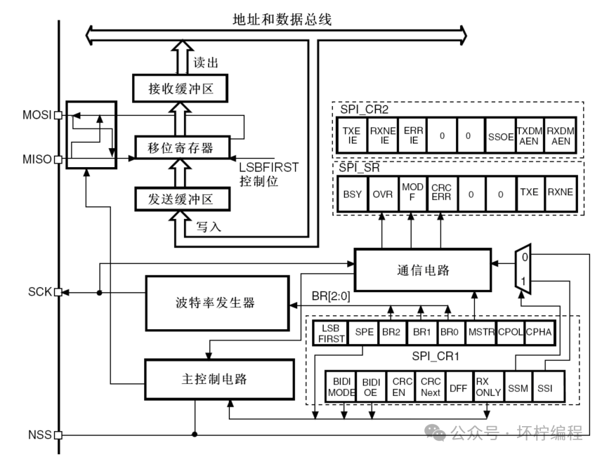 The device cooperates with MOSI and MISO along with the receive buffer and transmit buffer to perform complete data exchange. When data transmission is complete, the TXE signal is triggered. Since transmission and reception occur simultaneously, the RXNE signal is also received. These two signals indicate that the transmit buffer is empty and the receive buffer is not empty, respectively. At this point, we can read the data from the receive buffer and continue to transmit data to the transmit buffer.
Working Modes
Four working modes are formed by combining CPOL (Clock Polarity) and CPHA (Clock Phase)
Clock Polarity (CPOL):Idle state level of the clock line when no data is being transmitted
- 0: SCK remains low in idle state
- 1: SCK remains high in idle state
Clock Phase (CPHA):At which clock edge the data is sampled
- 0: Data bits are sampled on the first (odd) edge of SCK, data is latched on the first clock edge
- 1: Data bits are sampled on the second (even) edge of SCK, data is latched on the second clock edge
| Mode | CPOL | CPHA | Data Sampling Timing |
|---|---|---|---|
| 0 | 0 (low level initial) | 0 | First edge of SCK (rising edge) |
| 1 | 0 | 1 | Second edge of SCK (falling edge) |
| 2 | 1 (high level initial) | 0 | First edge of SCK (falling edge) |
| 3 | 1 | 1 | Second edge of SCK (rising edge) |
Timing Diagram for Mode 0: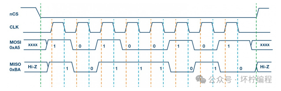 Timing Diagram for Mode 3:
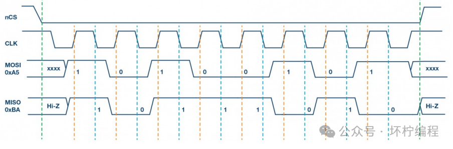
1.4 SPI Registers
SPI Control Register 1 (SPI_CR1) (Not used in I2S mode)
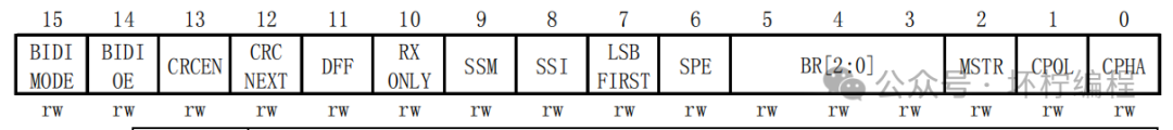
- Bit 15 – BIDIMODE: Bidirectional data mode enable
0: Select “Dual-line Bidirectional” mode;1: Select “Single-line Bidirectional” mode.
If we want to use half-duplex, we can set this bit to 1.
- Bit 11 – DFF: Data frame format
0: Use 8-bit data frame format for transmission/reception;1: Use 16-bit data frame format for transmission/reception.Note: This bit can only be written when SPI is disabled (SPE=0), otherwise an error will occur.
- Bit 9 – SSM: Software slave management
When SSM is set, the level on the NSS pin is determined by the value of the SSI bit.0: Disable software slave management;1: Enable software slave management.
When we want to specify a GPIO pin as a custom chip select port, we need to set this bit to 1.
- Bit 7 – LSBFIRST: Frame format
0: Send MSB first;1: Send LSB first.Note: This bit cannot be changed while communication is ongoing.
This is used to choose whether to transmit data in MSB first or LSB first mode.
- Bit 6 – SPE: SPI enable
0: Disable SPI device;1: Enable SPI device.
- Bits 5:3 – BR[2:0]: Baud rate control
000: fPCLK/2 001: fPCLK/4 010: fPCLK/8 011: fPCLK/16100: fPCLK/32 101: fPCLK/64 110: fPCLK/128 111: fPCLK/256These bits cannot be modified while communication is ongoing.
This is used for frequency division.
- Bit 2 – MSTR: Master selection
0: Configured as a slave device;1: Configured as a master device.
- Bit 1 – CPOL: Clock polarity
0: SCK remains low in idle state;1: SCK remains high in idle state.
- Bit 0 – CPHA: Clock phase
0: Data sampling starts from the first clock edge;1: Data sampling starts from the second clock edge.
SPI Control Register 2 (SPI_CR2)
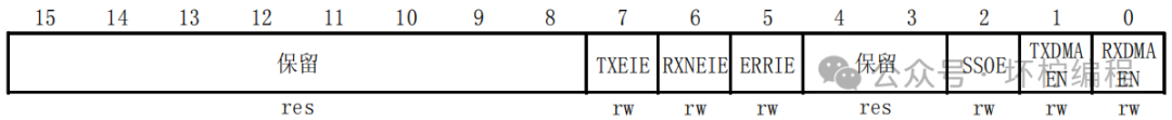
- Bit 7 – TXEIE: Transmit buffer empty interrupt enable
0: Disable TXE interrupt;1: Enable TXE interrupt, generates an interrupt request when the TXE flag is set to ‘1’.
- Bit 6 – RXNEIE: Receive buffer not empty interrupt enable
0: Disable RXNE interrupt;1: Enable RXNE interrupt, generates an interrupt request when the RXNE flag is set.
SPI Status Register (SPI_SR)
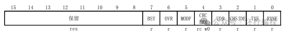
Focus on the following two bits:
- Bit 1 – TXE: Transmit buffer empty
0: Transmit buffer not empty;1: Transmit buffer empty.
- Bit 0 – RXNE: Receive buffer not empty
0: Receive buffer empty;1: Receive buffer not empty.
SPI Data Register (SPI_DR)

2. Common SPI Functions in HAL Library
2.1. Initialization Function
HAL_SPI_Init(SPI_HandleTypeDef *hspi);
Configures SPI working parameters (mode, speed, data width, etc.)
2.2. Data Transmission Functions
// Blocking send
HAL_SPI_Transmit(SPI_HandleTypeDef *hspi, uint8_t *pData, uint16_t Size, uint32_t Timeout);

// Blocking receive
HAL_SPI_Receive(SPI_HandleTypeDef *hspi, uint8_t *pData, uint16_t Size, uint32_t Timeout);

// Simultaneous send and receive
HAL_SPI_TransmitReceive(SPI_HandleTypeDef *hspi, uint8_t *pTxData, uint8_t *pRxData,
                       uint16_t Size, uint32_t Timeout);