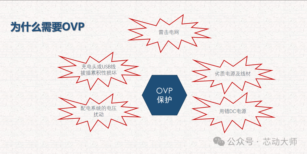
OVP (Over-Voltage Protection) chips are critical protective devices used in electronic systems to prevent input voltage from exceeding the rated value of the device. They are widely used in embedded systems, power modules, consumer electronics, and other scenarios (such as STM32 development boards, sensor modules, and power circuits for smart pet feeders/drinkers). Their core function is to quickly cut off the circuit or clamp the voltage when the input voltage rises abnormally, preventing damage to downstream chips (such as MCUs and sensors) from overvoltage.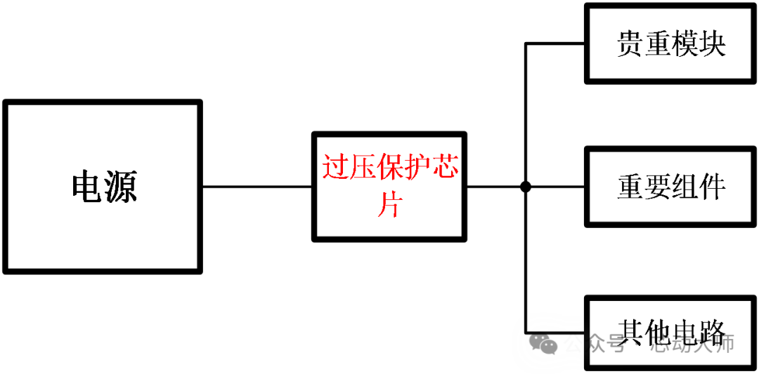
1. Core Components
The internal structure of OVP chips typically includes four key modules. Different models (such as TI’s TPS2491 and ON’s NCP361) may vary slightly, but the core principles are consistent:
| Module | Function Description |
|---|---|
| Voltage Detection Module | Real-time sampling of input voltage (VIN) and comparing it with the internal reference voltage (VREF) to determine if there is an overvoltage condition. |
| Reference Voltage Source | Provides a high-precision, stable reference voltage (such as 2.5V or 4.0V) as the “threshold standard” for overvoltage judgment. |
| Logic Control Module | Receives signals from the voltage detection module, triggers protective actions (cutting off the circuit/clamping voltage), and outputs fault signals. |
| Output Execution Module | Typically consists of MOSFETs or SCRs, executing “turn on/off” or “voltage clamping” operations. |
2. Core Working Principle (3-Step Process)
1. Voltage Sampling and Comparison
The OVP chip samples the input voltage (VIN) through internal voltage divider resistors (or external resistors) to obtain the sampled voltage (VSAMPLE).
- Sampling Voltage Formula:
<span>VSAMPLE = VIN × (R2 / (R1 + R2))</span>(where R1 and R2 are internal voltage divider resistors) - The chip compares
<span>VSAMPLE</span>with the internal reference voltage<span>VREF</span>in real-time: - When
<span>VSAMPLE ≤ VREF</span>(i.e.,<span>VIN ≤ Threshold Voltage VOV</span>): the circuit is normal, and the output execution module remains on, supplying normal voltage to the downstream load. - When
<span>VSAMPLE > VREF</span>(i.e.,<span>VIN > VOV</span>): it is determined to be overvoltage, triggering the protection mechanism.
2. Setting the Threshold Voltage (VOV)
The overvoltage protection threshold (VOV) is a core parameter determined by the reference voltage and voltage divider resistors:
<span>VOV = VREF × (R1 + R2) / R2</span>
- Fixed Threshold OVP Chip: R1 and R2 are internal fixed resistors, and VOV is not adjustable (e.g., VOV=5.5V for TPS2490).
- Adjustable Threshold OVP Chip: VOV can be modified by external voltage divider resistors (R1_ext, R2_ext) to adapt to different load requirements (e.g., for a 3.3V powered STM32 system, VOV can be set to 3.6V).
3. Execution of Protective Actions (Two Core Modes)
When overvoltage occurs, the OVP chip responds quickly through the output execution module, with two common protection modes:
(1) Cut-off Mode (Most Common)
- Principle: The logic control module outputs a shutdown signal, causing the internal MOSFET (or SCR) to turn off, disconnecting the input voltage from the load.
- Response Time: Typically in the ns to μs range (e.g., NCP361 has a response time of < 1μs), preventing instantaneous overvoltage from damaging the chip.
- Reset Method:
- Automatic Reset: After the overvoltage disappears and VIN returns below the threshold, the chip automatically turns on after a delay (typically 10-100ms) to restore power.
- Manual Reset: Requires re-powering or triggering the reset pin (RESET), suitable for scenarios needing manual fault diagnosis.
(2) Clamping Mode
- Principle: When VIN exceeds VOV, the internal clamping circuit (such as a Zener diode + MOSFET) activates, clamping the output voltage near VOV to prevent further voltage increase.
- Applicable Scenarios: Scenarios where the load cannot be instantly powered off (e.g., sensor data collection, continuous power supply for smart pet devices), but note that during clamping, the chip will consume excess power (adequate heat dissipation is required).
4. Auxiliary Functions (Optional)
- Under-Voltage Protection (UVP): Some OVP chips integrate under-voltage detection, cutting off the output when VIN falls below the under-voltage threshold (UVOV) to prevent the load from operating abnormally at low voltage.
- Over-Current Protection (OCP): Combined with over-current detection to prevent excessive current caused by short circuits or overloads.
- Fault Output (FLAG): Outputs a low/high signal during overvoltage, notifying the MCU (such as STM32) to log the fault or trigger an alarm (e.g., LED blinking).
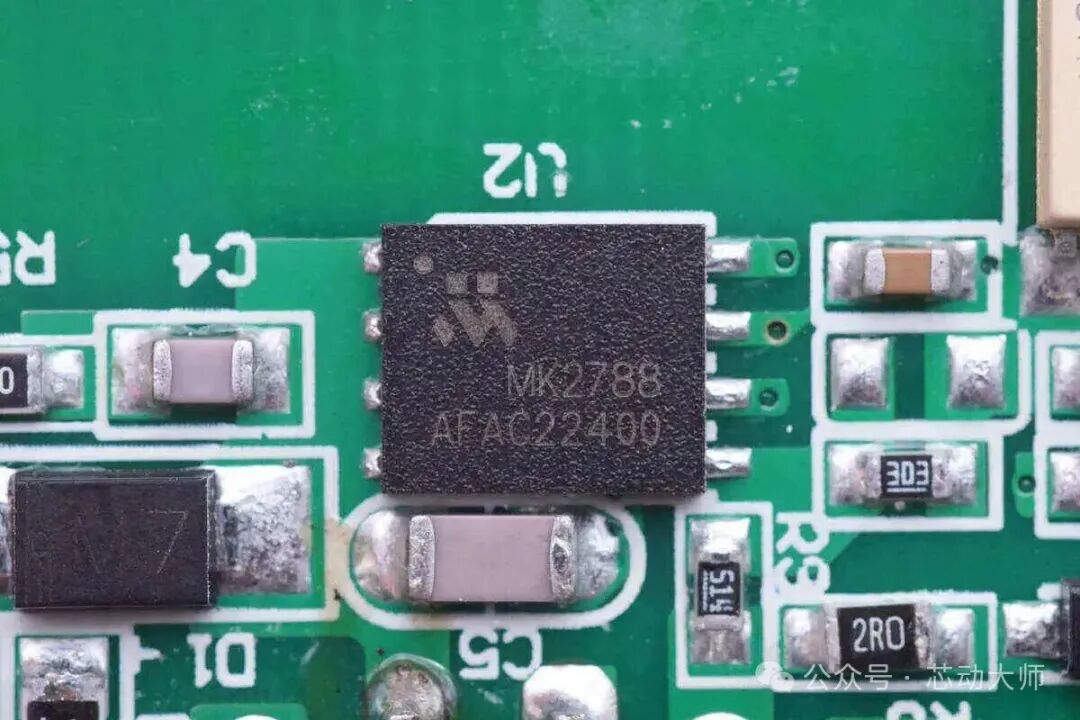
3. Typical Applications in Embedded Systems (Taking STM32 as an Example)
1. Application Scenarios
The rated supply voltage for STM32 microcontrollers is typically 3.3V (allowable range 2.0V-3.6V). If the external power supply (such as a lithium battery or adapter) fluctuates (e.g., suddenly rising to 5V), an OVP chip is needed to protect the core circuit of the STM32.
2. Code-Level Coordination (STM32 Example)
If the OVP chip has a fault output (FLAG pin), the fault status can be detected through the GPIO port of the STM32 to implement alarms or log records:
#include "stm32f10x.h"#define OVP_FLAG_PIN GPIO_Pin_0#define OVP_FLAG_PORT GPIOAvoid GPIO_Configuration(void) { GPIO_InitTypeDef GPIO_InitStruct; RCC_APB2PeriphClockCmd(RCC_APB2Periph_GPIOA, ENABLE); // Configure OVP_FLAG_PIN as input mode (pull-up) GPIO_InitStruct.GPIO_Pin = OVP_FLAG_PIN; GPIO_InitStruct.GPIO_Mode = GPIO_Mode_IPU; // Pull-up input, high level when no fault GPIO_InitStruct.GPIO_Speed = GPIO_Speed_50MHz; GPIO_Init(OVP_FLAG_PORT, &GPIO_InitStruct);}int main(void) { GPIO_Configuration(); while(1) { // Detect OVP fault (FLAG pin pulled low indicates overvoltage) if(GPIO_ReadInputDataBit(OVP_FLAG_PORT, OVP_FLAG_PIN) == RESET) { // Execute fault handling: light up alarm LED, log fault, enter low power mode, etc. GPIO_SetBits(GPIOB, GPIO_Pin_0); // Assume PB0 is connected to alarm LED // Optional: Send fault information to the host via serial port USART_SendString(USART1, "OVP Fault: Over-Voltage Detected!\r\n"); } else { GPIO_ResetBits(GPIOB, GPIO_Pin_0); // Turn off LED when no fault } }}4. Key Parameter Selection Considerations
- Threshold Voltage (VOV) should be slightly higher than the maximum rated voltage of the load (e.g., for a 3.3V system, choose 3.6V; for a 5V system, choose 6.0V) to avoid false triggering due to normal voltage fluctuations.
- Response Time In embedded systems, prioritize chips with response times < 1μs to handle instantaneous overvoltage (e.g., caused by power plug/unplug or electrostatic interference).
- Maximum Operating Current must be greater than the total load current (e.g., for STM32 + sensor total current of 500mA, choose an OVP chip with a maximum current of over 1A).
- Static Current (IQ) In low-power scenarios (e.g., battery-powered smart pet devices), choose chips with IQ<1μA to extend battery life.
- Protection Mode Choose “cut-off mode” if the load can be powered off, and “clamping mode” if continuous power supply is required.
Conclusion
The core logic of OVP chips is **”Voltage Sampling → Threshold Comparison → Rapid Protection”**, providing the first line of overvoltage protection for embedded systems and hardware modules through real-time monitoring and response at the hardware level. In actual development, it is essential to select the appropriate OVP chip based on load voltage, current, and power requirements, along with voltage divider resistors and software fault detection, to ensure system stability (such as in scenarios requiring high reliability like smart pet devices and industrial sensors).