
Chips are one of the greatest inventions of our time. Without the advent of chips, it is hard to imagine what today’s electronic era would look like. Everyone operates a “computer” the size of a house, carrying a huge “phone” while talking to friends far away, and the sound quality is terrible. It is precisely because of the invention of chips that all functions are concentrated in a tiny chip the size of a fingernail, allowing ordinary people to truly enjoy the convenience brought by this wireless era. However, to this day, chips still remain a bottleneck. So today, let’s learn about the knowledge related to chips.
What is a Chip?
A chip, also known as an integrated circuit or very-large-scale integration (VLSI), is an electronic circuit composed of thousands, millions, or even billions of transistors, resistors, and capacitors. It performs the same functions as a larger circuit built using discrete (individually packaged) components, but an IC is an extremely compact device built as a single unit on a small piece of semiconductor material. The primary raw material used to manufacture ICs is silicon; therefore, ICs are often referred to as “silicon chips.” Other materials, such as germanium and gallium arsenide, can also be used, but silicon is the primary choice for the following reasons:
-
Silicon is a semiconductor, which means it can act as a conductor and insulator under certain controlled conditions in a process known as doping. Doping refers to adding impurities to change the electrical characteristics of the element.
-
Silicon is abundant on Earth, making it very affordable.
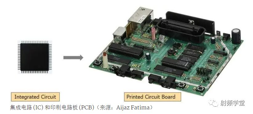
Chips are designed for specific purposes and can be used in various industries, such as aerospace, automotive, telecommunications, computing, and more. One or more ICs, along with other components and connectors, are mounted on a printed circuit board (PCB) and connected with fine copper traces to meet application requirements. A very common use of PCBs is as the motherboard of a computer.
Classification of Chips
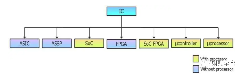
ASIC is an acronym for Application Specific Integrated Circuit, which refers to ICs designed for specific applications, mainly used in electronic devices such as routers, switches, and modems.
The main features of ASICs are as follows:
-
Performs the same function throughout its entire lifecycle -
No processor -
Design cycle is time-consuming and costly -
Mass production -
High speed and low power consumption -
Can be digital, analog, or both
ASSP stands for Application Specific Standard Part, which is designed for specific applications but not customized for systems or customers. ASSP is a special type of ASIC that can be used by multiple companies. The characteristics of ASSP are similar to those of ASICs. It is mainly used in Ethernet controllers, PCIe controllers, USB interfaces, etc.
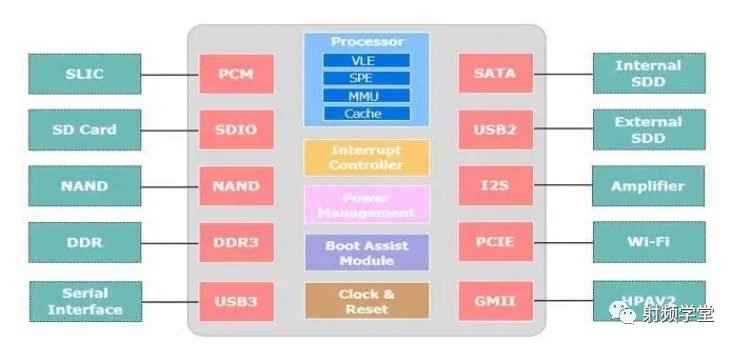
SoC (System on Chip): An IC that integrates a complete system is called a SoC. It includes processors, memory, peripherals, and software. The processor in a SoC can be a microprocessor (μP or MPU), microcontroller (μC or MCU), digital signal processor (DSP), or graphics processor. ASICs or ASSPs with processors are SoCs, so the characteristics of SoCs are similar to those of ASICs or ASSPs. They are mainly used in voice, video, and image signal processing, wireless communication, automotive applications, etc.
FPGA (Field Programmable Gate Array): An FPGA is a programmable IC. It has configurable logic blocks, configurable input-output blocks, and programmable interconnections. It is mainly applied in prototyping ASICs or SoCs, device controllers, signal processing systems, image processing systems, etc. The main features of FPGAs are as follows:
-
Suitable for designs that require frequent customization
-
No processor
-
Design cycle is not time-consuming and cost-effective
-
Suitable for small size designs
-
Lower speed and low power consumption
Programmable SoC or SoC FPGA: An IC that integrates a processor and FPGA architecture is called a programmable SoC or SoC FPGA. This also includes peripherals, on-chip memory, FPGA-style logic arrays, and high-speed transceivers. They are mainly used in networking, aerospace, defense, etc. The main features of programmable SoCs/SoC FPGAs are as follows:
-
Suitable for designs that require frequent customization and processing capabilities
-
Smaller size
-
Higher bandwidth communication between the processor and FPGA
-
Design cycle is not time-consuming and cost-effective
-
Low risk because it is reprogrammable
-
Lower speed and low power consumption
Microprocessor (μP or MPU): An IC that contains only a processor is called a microprocessor. It does not include memory (RAM, ROM, etc.) or any other peripherals. The main characteristics of microprocessors are:
-
Expensive
-
Higher speed and higher power consumption
-
Suitable for larger designs
-
Executes complex tasks
Applications: Desktop computers, laptops, notebooks, cars, trains, etc.
Microcontroller (μC or MCU): An IC that contains a processor as well as memory (RAM, ROM, etc.) and other peripherals is called a microcontroller. It is a general-purpose device that needs to be programmed for applications. Microcontrollers can be used in various industrial products. Microcontrollers are a scaled-down version of SoCs. The main characteristics of microcontrollers are:
-
Compact, as all peripherals are on the IC
-
Contains a processor
-
Cheaper than microprocessors
-
Lower speed and low power consumption
-
Suitable for smaller designs because it is compact
-
Executes less complex tasks
Applications: Microwave ovens, washing machines, DVD players, mobile phones, etc.
How are Chips Designed?
The diagram below reflects the IC design cycle (the following sections explain each step):
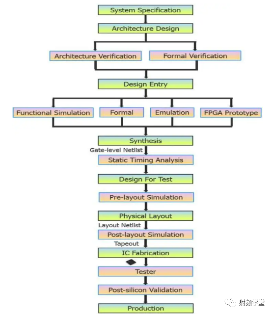
IC vendors meet with potential customers to determine the functions they are looking for and prepare a list of functional requirements. The system specification is the process of specifying the functional specifications (or requirements) of the system (IC) and defining its external interfaces.
Once the system specifications are determined, the architecture design process begins. This includes creating or purchasing intellectual property (IP) blocks and defining software interfaces, timing, performance, area, and power constraints. Standard industrial IP modules can be obtained from IP vendors.
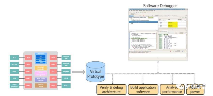
Architecture verification is the process of building a software version of the hardware system. This is created from a functional model using high-level languages (such as C, C++, or SystemC). The architecture, performance, and power of the entire system are evaluated using software debuggers.
Formal Verification / Property Checking
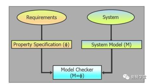
Formal verification is the process of statically verifying the correctness of the design using mathematical methods without using any stimuli or timing checks.
A formal verification method called property checking is used to prove that the implemented system model meets the design requirements (or specifications). In property checking, property specification languages (such as PSL and SVA) are used to define system requirements, and a mathematical model of the implemented system is created. A model checker is used to compare the system requirements and the mathematical model to confirm that the system meets the requirements.
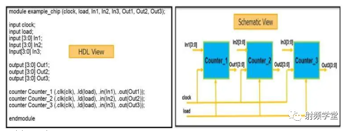
Design Input
After the system architecture design and verification, the next step is design input. This is the process of capturing the complete system design using hardware description languages (HDL) (such as VHDL and Verilog) and/or schematic capture. The design includes details of I2C input and output pins, IP block instances, design connections, clock, and reset strategies.
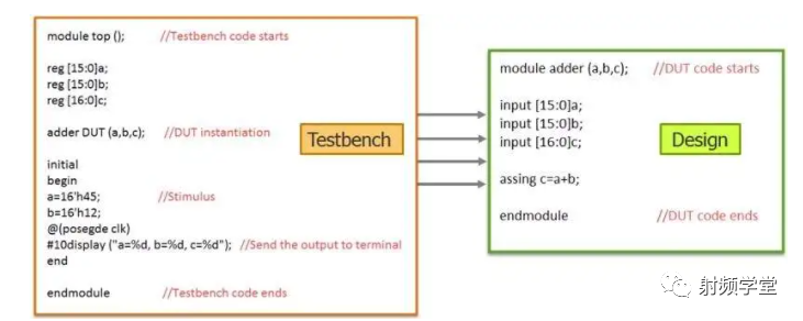
Functional Simulation
Functional simulation is the process of verifying the functional behavior of the design using software simulators. Timing delays of design elements are not considered. It verifies IC-level connectivity, IP blocks in the IC-level environment (general IP blocks are pre-validated), end-to-end functional paths, pad connectivity, module interactions, external module interactions, etc.
The testbench is a set of code used to check whether the RTL implementation meets (or does not meet) the design specifications. It includes valid and expected conditions as well as invalid and unexpected conditions to check if the design operates as expected.
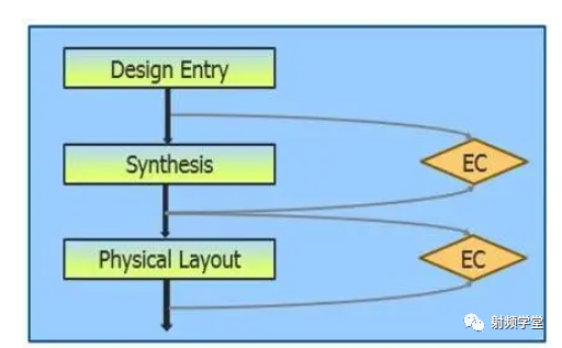
Formal Verification – Equivalence Checking
As previously mentioned, formal verification is the process of statically verifying the correctness of the design using mathematical methods without using any stimuli or timing checks.
A formal verification method called equivalence checking is used to find the functional equivalence of the design by comparing it with a golden design. The diagram below describes the equivalence checking at various stages of the IC design cycle:
Silicon Validation
Silicon validation is the process of verifying the design in hardware before sending it to manufacturing. It can validate high-risk or newly developed IP and save costs on re-spins of ICs. Silicon validation can be performed using simulators or FPGAs.
Benefits:
-
Very fast compared to a simulated environment
-
Can probe a limited set of internal signals for debugging
-
Can validate software and application-level scenarios before tape-out
Limitations:
-
Hardware is expensive
-
Cannot validate analog IP blocks
-
System clock speeds are slower compared to real chips
-
Requires multiple hardware setups, especially when validation and software teams are distributed across multiple geographical locations
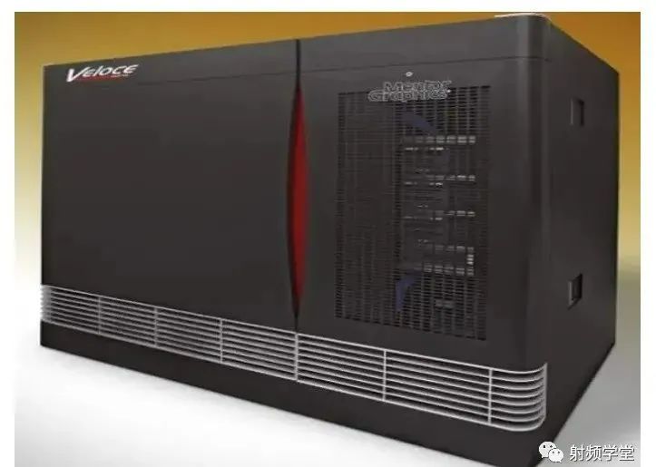
Simulation
Simulation is the process of verifying system functionality on a hardware device called a simulator. Simulators can run very large IC designs faster than simulations and can run many IC designs at different clock speeds simultaneously. The diagram below shows the state-of-the-art simulators:
FPGA-Based Prototyping
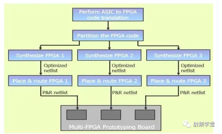
FPGA-based prototyping is the process of verifying system functionality using one or more FPGAs. The FPGA prototyping follows these steps:
-
Convert ASIC RTL (Register Transfer Level) code to FPGA RTL code. This includes using different memory, removing analog blocks, rewriting clock schemes, etc.
-
If the complete FPGA RTL code does not fit into a single FPGA, the code is partitioned across multiple FPGAs.
-
FPGA tools are used for synthesis and place-and-route.
-
The bit file is downloaded into the FPGA and the design is verified.
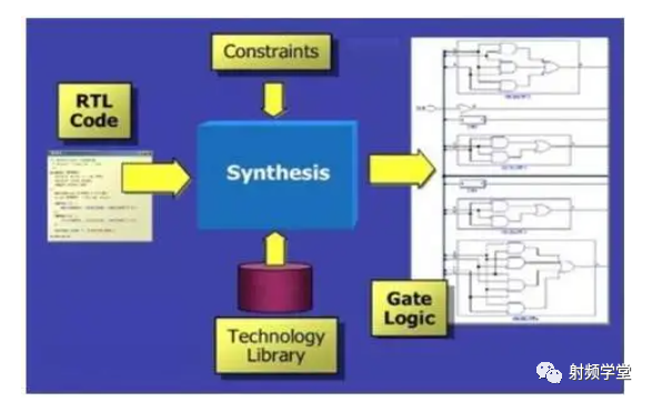
Synthesis
Synthesis is the process of converting the RTL code of the design into an optimized gate-level representation under a given technology library and design constraints. The following steps are performed in synthesis:
-
Translation: The design RTL code is translated into technology-independent Boolean equations.
-
Optimization: The Boolean equations are optimized to remove redundant logic.
-
Technology Mapping: The technology-independent Boolean equations are mapped to technology-specific logic gates with the help of design constraints and technology libraries.
Static Timing Analysis (STA)
Static Timing Analysis (STA) is the process of verifying the timing characteristics of the design without providing any stimuli. STA is quick and thorough, but it does not check the functionality of the design. Electronic devices are driven by clock signals; therefore, it must be verified that the design operates at the specified clock frequency. STA is performed at various stages of the IC design cycle.
Design for Test (DFT)
The process of manufacturing ICs is not 100% error-free. Therefore, additional logic called Design for Test (DFT) logic must be inserted into the design to assist in post-production testing of the IC to identify manufacturing defects. During IC manufacturing, any manufacturing defects are first checked with the help of DFT logic. If no manufacturing defects are found, the functionality of the IC is then checked.
Pre-Layout Simulation
Before sending the gate-level netlist for physical layout, software applications verify its functionality and timing behavior. This is called pre-layout simulation.
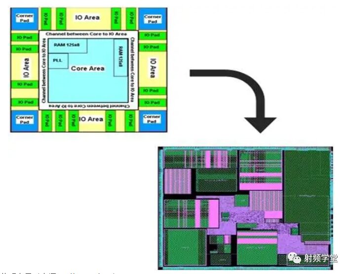
Physical Layout
Physical layout is the transition from the logical view of the IC to the physical view. The output of the physical layout process is a graphic database system (GDSII) file, which is a binary file format representing planar geometric shapes, text labels, and other information related to the physical layout. The steps performed in physical layout are as follows:
-
Layout Planning: Determine the main design blocks and allocate space to meet timing, area, and performance standards. The IP structure, aspect ratio, and routing possibilities are also determined here.
-
Partitioning: Divide the IC into functional blocks to facilitate layout and routing.
-
Layout Routing: Place and connect design blocks without violating design rules.
-
Clock Tree Synthesis: Clocks are evenly distributed to all timing elements in the design.
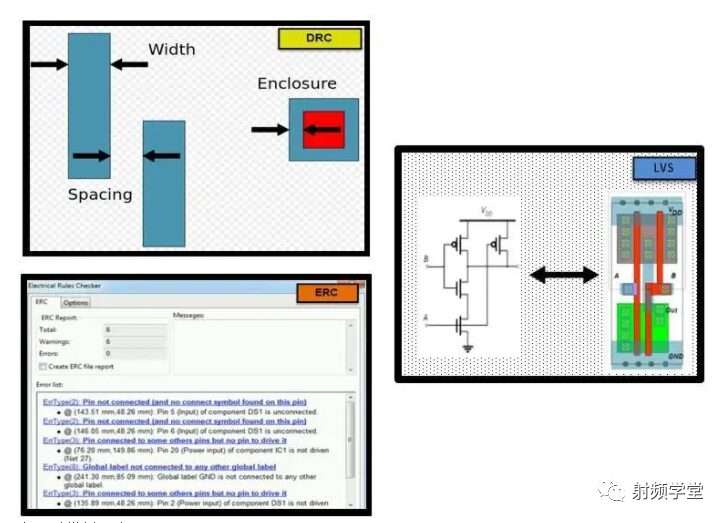
Post-Layout Simulation
Post-layout simulation is the process of verifying the design after the physical layout of the design has been established. The checks performed in post-layout simulation are as follows:
-
Design Rule Check (DRC): The layout meets a set of rules required for manufacturing.
-
Electrical Rule Check (ERC): The layout meets a set of electrical design rules.
-
Layout versus Schematic (LVS): The layout is functionally the same as the netlist of the design.
Integrated Circuit Manufacturing
After post-layout simulation, the layout netlist in GDSII file format is provided to the IC manufacturer (foundry). The process of providing the GDSII file to the foundry is known as tape-out. The IC manufacturing process is illustrated in the diagram below:
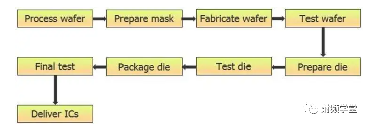
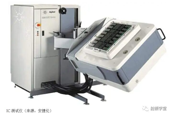
IC Tester
The manufacturing of ICs is not 100% reliable, leading to many samples having manufacturing defects. Once ICs are received from the foundry, testers are used to filter out defective ICs. The tester provides input stimuli to the IC and verifies the output. It also verifies the electrical and thermal characteristics of the IC and finds ideal operating conditions.
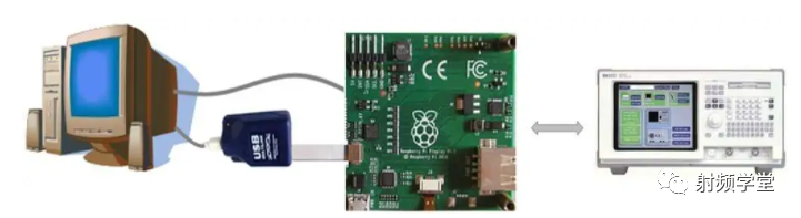
Post-Silicon Validation
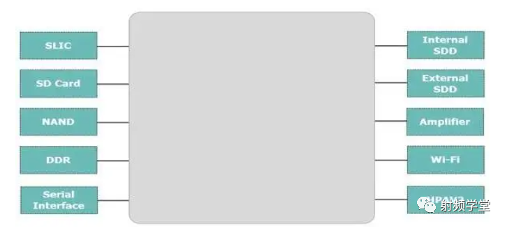
Samples that pass the tester are validated in a real environment. This is called post-silicon validation. In post-silicon validation, software tools on a computer configure the IC and download test code into the IC. The expected output is monitored, and all functionalities of the IC are validated. The diagram below describes the validation setup:
Summary
There are various types of ICs, each with specific characteristics: programmable or non-programmable, with or without processors, high-speed or low-speed, compact or bulky. The process of designing, manufacturing, and testing ICs is complex and detailed. The main contributors are the design and verification teams, IP vendors, and IC manufacturers. Advanced EDA tools play a crucial role in reducing the time and effort associated with the IC design cycle.
References
-
https://anysilicon.com/ic-design-flow-an-overview/ -
https://www.synopsys.com/glossary/what-is-ic-design.html -
https://byjus.com/physics/integrated-circuit/ -
https://www.allaboutcircuits.com/technical-articles/basics-of-ic-design-flows/ -
https://diaridelsestudiants.com/what-is-digital-integrated-circuit-design/ -
https://www.eeweb.com/introducing-the-integrated-circuit-ic-design-cycle/


E课网(www.eecourse.com) is a professional integrated circuit education platform under Moore Elite, dedicated to cultivating high-quality integrated circuit professionals in the semiconductor industry. The platform is oriented towards the job requirements of integrated circuit enterprises, providing a practical training platform that fits the corporate environment, and rapidly cultivating students to meet corporate needs through online and offline training methods.
E课网 has a mature training platform, a complete curriculum system, and a strong faculty, planning 168 high-quality semiconductor courses in China, covering the entire integrated circuit industry chain, and has 4 offline training bases. To date, it has deeply cultivated a total of 15,367 people, directly supplying 4,476 professionals to the industry. It has established deep cooperative relationships with 143 universities and has held 240 corporate-specific IC training sessions.