Integrated Chips are technologies that integrate several chiplets through semiconductor micro-nano processes to create chips and systems with higher integration and richer functions than single chips.
As the development of Moore’s Law gradually slows, integrated chips and chiplet technologies are playing an increasingly important role in the manufacturing and design of high-performance chips, serving as a crucial engine for accelerating the construction of a technologically strong nation and achieving high-level technological self-reliance.
Against the backdrop of the National Natural Science Foundation’s deployment of major research plans for integrated chips, the first Integrated Chip and Chiplet Conference was successfully held in Shanghai, co-hosted by Fudan University and the Institute of Computing Technology, Chinese Academy of Sciences, with the theme of “Interdisciplinary Exploration of Frontier Technologies in Integrated Chips.”
The conference chairman, Academician Sun Ninghui of the Chinese Academy of Engineering and the Institute of Computing Technology, Chinese Academy of Sciences, delivered an important report at the conference, reviewing the development history of integrated chips, summarizing the scientific problems faced by integrated chips, and forecasting the trends in the development of integrated chips.
01
Development History of Integrated Chips
The original intention of developing integrated chips was to meet the demands of supercomputing. Academician Sun Ninghui pointed out that the development of computers and chip technology has almost corresponded one-to-one: the basic semiconductor components have undergone transitions from vacuum tubes to discrete transistors, planar integrated transistors, ultra-large-scale integrated transistors, and 3D integrated transistors, leading to a surge in computing power, from initially only 385 FLOPS low-power computers to supercomputers exceeding 1000 PFLOPS.
Academician Sun mentioned that he hopes to develop Z-level computers by 2035. What are the chip foundations required for such computing systems? This question has become a significant driving force for the development of next-generation semiconductor technologies.
02
Three Main Technical Paths to Enhance Chip Performance
Academician Sun Ninghui summarized the three main technical paths currently enhancing chip performance, which complement each other and jointly promote chip upgrades and iterations.
1. Classic Moore’s Law
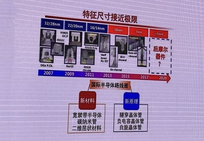
Currently, increasing integration through transistor size reduction remains the main line of development. The performance of single-die CPUs is constrained by the photolithography area and process nodes; under the same chip area, the process node is a decisive factor for computing power. However, the current international advanced process sizes are approaching physical limits, technological development is slowing, and China still faces restrictions from the lithography machine ban, making it challenging to break through the EUV lithography bottleneck and achieve processes under 7nm. Additionally, increasing CPU performance by expanding multi-core scale is limited by yield.
2. New Principle Devices
As Moore’s Law gradually slows, developing new principle devices and researching new materials to enhance the performance of individual transistor devices is becoming a consensus in the industry. Academician Sun pointed out that new principle devices are currently limited to application computing in specialized high-end fields, and due to the long cycle from research to application, they need to be deployed in advance. In 2019, the National Natural Science Foundation launched a major research plan for “New Devices in the Post-Moore Era,” promoting fundamental research and architectural innovation for new devices in a comprehensive manner from device electronics, new physical mechanisms, new material systems, and bionic electronics.
3. Integrated Chips
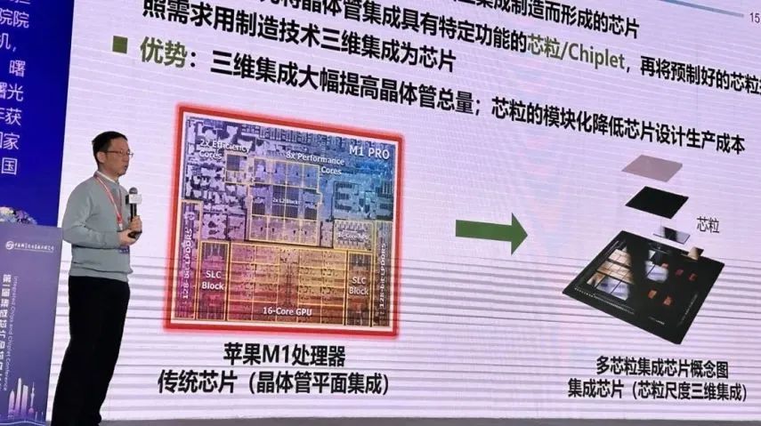
Academician Sun stated that from the perspective of computing systems, scaling up can occur not only at the microscopic circuit level but also at the terminal chip level. Traditional chips are manufactured by integrating a large number of transistors on a two-dimensional plane, while integrated chips first integrate transistors into chiplets with specific functions, and then use manufacturing technologies to three-dimensionally integrate the prefabricated chiplets as needed. The advantage of this approach is that it can significantly increase the total number of transistors, and the modularity of chiplets can reduce the design and production costs of chips.
Integrated chips represent a transformative technological approach to achieving high-performance chips using existing independent processes, for example, achieving the performance of 7nm or even 5nm chips using 14nm processes, which can alleviate the current demand crisis and complement the other two paths.
The existing chip design paradigm is a bottom-up stacking from transistors to chips, which comes with two inherent problems: one is the ever-increasing design complexity due to the massive number of transistors, and the second is that the industry is easily dominated by manufacturers mastering advanced process technologies. Integrated chips will bring about a transformation in the chip design paradigm. Academician Sun emphasized that the shift from the “stacking method” to the “constructive method” reflects a change in complex systems. The “constructive method” of integrated chips introduces the concept of systems engineering, decomposing, combining, and integrating from the top down, which will significantly reduce design difficulty.
03
Scientific Issues of Integrated Chips
The significant increase in chiplet integration brings about new scientific issues.
1. Mathematical Description and Combination Optimization Theory of Chiplets
When integrating a small number of chiplets, the mapping relationship is simple, but when decomposing complex functions into a large number of chiplets, mathematical operations are needed; the traditional mathematical description for micro-transistors in integrated circuits is not applicable at the chiplet scale, necessitating the establishment of new mathematical theories. Academician Sun’s research approach differs from the traditional Boolean algebra representation of transistor functions in chips, using function theory to abstractly describe multi-chiplet systems and establishing modeling and analysis for optimal decomposition of chiplets in integrated chips based on complex function decomposition optimization.
Academician Sun mentioned that attention should be focused on the following three aspects:
-
Abstract Mathematical Description of Integrated Chips
-
Modeling, Dimensional Reduction, and Optimization Theory for Complex Design Spaces
-
Optimization of Cross-Level, Stochastic, and Inexact Computational Functions
2. Large-Scale Chiplet Parallel Architecture and Design Automation
As the number and variety of chiplets increase significantly, how to address the explosive growth in design complexity becomes a crucial issue. Currently, integrated chips have few types and numbers of chiplets, with limited adjustable design parameters, making parallel design relatively easy, but with large-scale chiplet integration, new issues such as decomposition efficiency and three-dimensional automated layout routing need to be considered, requiring EDA tools to address.
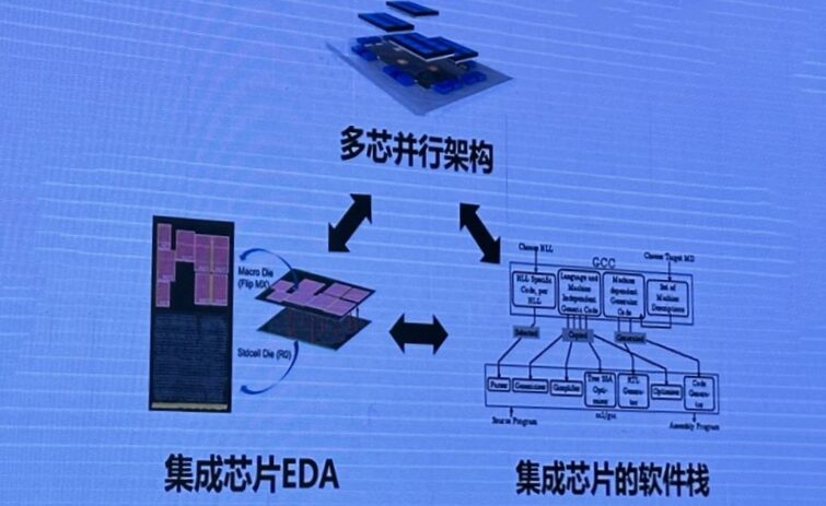
Academician Sun pointed out that existing EDA tools for planar circuit design based on transistors can serve as a foundation for developing three-dimensional EDA based on chiplets. Current commercial EDA tools mainly implement automation based on model/brute-force search methods. For integrated chips, new methods combining expert knowledge and artificial intelligence can replace traditional methods, constructing multi-chip architectures and optimization algorithms for integrated chip EDA tools to enhance design efficiency. In this regard, Academician Sun emphasized the importance of focusing on multi-chip parallel architectures and interconnection interfaces, comprehensive algorithms for integrated chips, layout routing algorithms, and compilation principles and software stacks for multi-chip parallelism.
3. Multi-Physical Field Coupling Mechanisms and Interface Theories at the Chiplet Scale
Academician Sun stated that when integrating a small number of chiplets, it is sufficient to analyze electrical, thermal, and mechanical conduction at a two-dimensional level, where the coupling degree is low due to distance, and effects are easy to predict. However, with large-scale chiplet integration extending into three-dimensional space, complex physical quantity transmission and coupling issues arise at the interfaces of multilayer stacked structures, and the physical models established for micro-transistor electrical, thermal, and mechanical conduction in traditional integrated circuits are no longer suitable for predictive analysis at the chiplet scale. Therefore, optimizing electrical and thermal conduction and avoiding stress damage at the interfaces formed by different functions and types of chiplets is the third major scientific issue faced by integrated chips.
The research approach mentioned by Academician Sun is that chiplets should serve as the core hub connecting the micro and macro levels, building rapid and precise simulation computing methods for multi-physical fields and multi-interface coupling at the chiplet scale based on micro-physical theories. In this process, attention should be paid to the multi-physical field simulation of electrical-thermal-stress interactions, power management and thermal theory for high-power integrated chips, and the reliability and fault-tolerant design of 3D interconnection interfaces.
04
Trends and Current Status of Integrated Chip Development
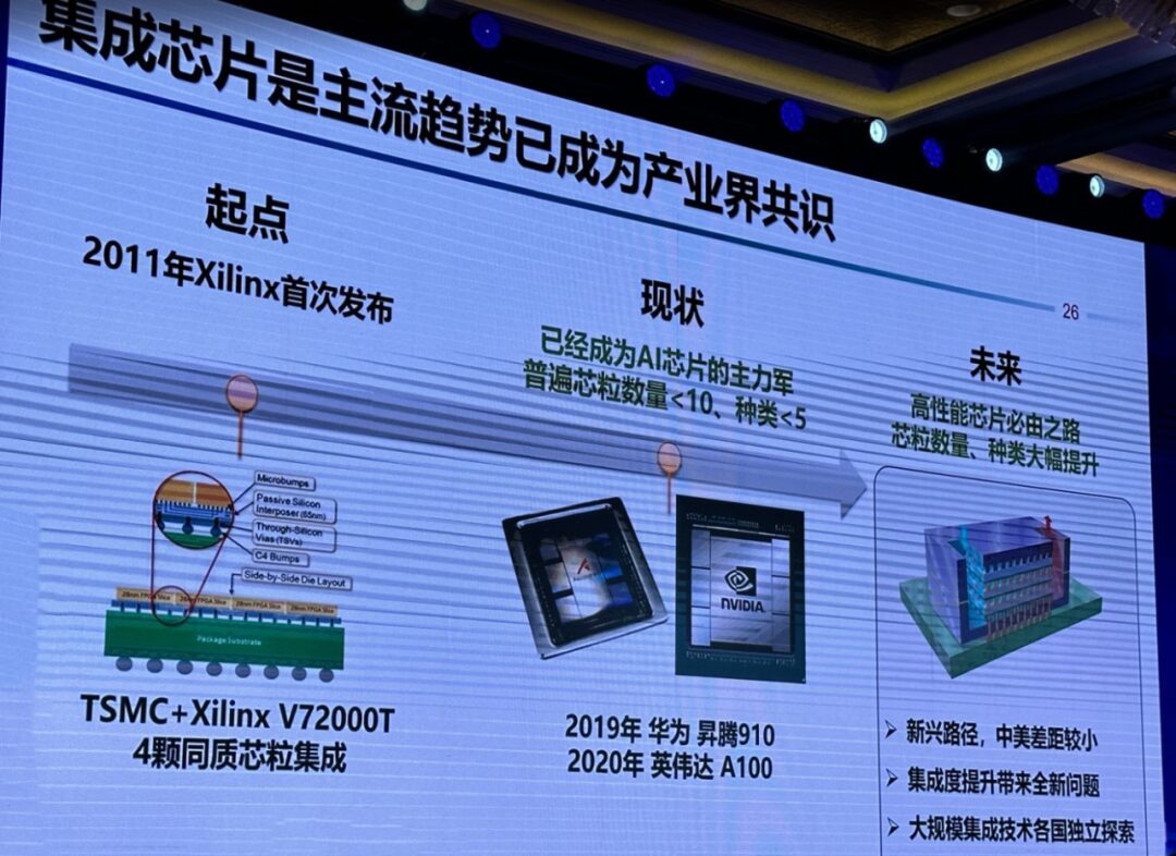
In the final part of his speech, Academician Sun mentioned that currently, integrated chips have become the mainstream trend in chip architecture, which is a consensus in the industry. In this emerging path, the gap between China and the US is relatively small, and countries are independently exploring the new issues arising from enhanced integration. The formulation of interconnection and interface standards is a current focus for the industry and an important cornerstone for building the integrated chip ecosystem. China is still in a relatively weak position in global ecosystem construction, so it needs to build an open and open-source chip ecosystem.
In July 2023, the National Natural Science Foundation launched a major research plan for “Scientific Foundations of Frontier Technologies in Integrated Chips,” aiming for continuous enhancement of integration scale, guided by scientific issues, and addressing technical challenges raised by enterprises, releasing a white paper and formulating a roadmap, stating that anything that can be open-source should be open-source, and establishing a unified open-source ecosystem. Academician Sun expressed that the scientific research of integrated chips needs to closely integrate with the business sector, where enterprises propose questions and academia provides answers, while also requiring technical personnel with interdisciplinary backgrounds in microelectronics, semiconductors, computers, materials, and mathematics to conduct research on integrated chip technologies together.
The major research plan for “Scientific Foundations of Frontier Technologies in Integrated Chips” focuses on the new issues arising from the significant increase in chiplet integration, requiring the convergence of wisdom from various fields, leveraging each other’s strengths, and facilitating extensive communication and collaboration to develop a new technological path for enhancing chip performance based on independent integrated circuit processes.
Source: Crystal Alliance
Image Source: The First Integrated Chip and Chiplet Conference
Disclaimer: We respect originality and emphasize sharing; the text and images are owned by the original authors. The purpose of reprinting is to share more information and does not represent our position. If your rights are infringed, please contact us promptly, and we will delete it immediately. Thank you!