This article introduces the principle of chip tape-out and the success of the first ultra-large-scale asynchronous circuit chip tape-out.
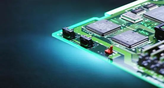
Chip tape-out is the process of manufacturing chips through a series of process steps, much like an assembly line.
Tape-out: In English, Tape Out. In the field of integrated circuit design, “tape-out” refers to “pilot production”. This means that after the circuit design is completed, a few chips are produced for testing. If the tests pass, then large-scale production begins based on this design.
We manufacture chips through a series of process steps like an assembly line, which is what tape-out is. In the chip manufacturing process, there are generally two time periods that can be referred to as tape-out.
During large-scale chip production, the assembly line-like production is one of them. Many may already be aware that this process is called tape-out. While we are designing, we may find areas that can be modified for better results, but we fear that such modifications may lead to unforeseen consequences for the chip. If chips are mass-produced based on such a problematic design, the losses could be significant. Therefore, to test whether the integrated circuit design is successful, tape-out must be performed, i.e., going from a circuit diagram to a chip, verifying whether each process step is feasible, and whether the circuit possesses the desired performance and functionality.
If the tape-out is successful, large-scale chip manufacturing can commence; otherwise, we need to identify the reasons and make corresponding optimization designs.
Why Is Chip Tape-Out So Expensive?
This brings us to the principles of chip manufacturing.
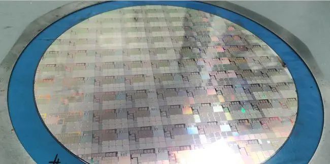
Chip manufacturing requires placing billions of transistors on a very small chip, and the manufacturing process has reached the nanometer level, which can only be completed using photolithography. Photolithography is the process of using light to create the desired patterns, and it requires a mask (also known as a photomask), which engraves the designed circuit diagram onto it, allowing light to pass through and etch the patterns onto the wafer.
The high cost of tape-out is partly due to the numerous processes that need to be validated. From a circuit diagram to a chip, we must verify whether each process step is feasible and whether the circuit meets the desired performance and functionality. The tape-out process typically lasts at least three months (including material preparation, photolithography, doping, electroplating, and packaging tests), generally involving over 1000 process steps, making it a crucial and costly phase in chip manufacturing.
If the tape-out is successful, large-scale chip manufacturing can be based on it; otherwise, the reasons must be identified, and corresponding optimization designs must be made.
Among them, the high cost of chip tape-out mainly lies in the photomask and the wafer, both of which are expensive consumables. The photomask is the most expensive, with a mid-range process photomask costing about $500,000, while a single wafer can also cost several thousand dollars.
A chip development project requires a long process from product definition, design, validation, simulation to final tape-out. As the “ultimate test”, any small oversight in the preceding lengthy process could lead to tape-out failure, and once tape-out fails, it often means that the company will face losses starting from tens of millions of dollars and a missed market opportunity of at least six months.
The First Ultra-Large-Scale Asynchronous Circuit Chip Tape-Out Success
This involves 120 chips named LZU_GERM. These chips use a 40-nanometer process and integrate 350 million transistors and 1512 CPUs on each chip, with a power consumption of only 98 milliwatts per chip. These chips completed their design at the end of April 2021 and successfully returned in May 2022.
 The advantages of asynchronous circuits mainly lie in low power consumption, while the challenge is the absence of a clock circuit as the global driving circuit for the chip. Moreover, mainstream commercial EDA software is designed for synchronous circuit design. There are many excellent synchronous circuit design teams in the country, but very few teams specialize in asynchronous circuit design, and even fewer have the capability to produce chips. Foreign countries have recognized the advantages of asynchronous circuits and started research early on, but there is a strict technology blockade against China. Based on mainstream commercial EDA software, significant breakthroughs have been made in asynchronous driving logic design, asynchronous timing constraints, large-scale asynchronous circuit design, and design stability verification.
Using the most advanced asynchronous circuit design methods internationally, each asynchronous CPU core on these small chips will be connected by an asynchronous mesh network, and data will be broadcast to various routing nodes after computation in the CPU, being captured by the target routing nodes. This working mechanism is very suitable for the brain-like computing and other high-concurrency computing fields that are very familiar to everyone today. In foreign countries, companies like Intel and IBM have already proven the use of asynchronous circuits for brain-like computing with chips like Loihi and TrueNorth, which outperform synchronous circuits of the same period in terms of both power consumption and performance. However, large-scale asynchronous circuit design in China is still in its initial stages, with great potential for the future.
The advantages of asynchronous circuits mainly lie in low power consumption, while the challenge is the absence of a clock circuit as the global driving circuit for the chip. Moreover, mainstream commercial EDA software is designed for synchronous circuit design. There are many excellent synchronous circuit design teams in the country, but very few teams specialize in asynchronous circuit design, and even fewer have the capability to produce chips. Foreign countries have recognized the advantages of asynchronous circuits and started research early on, but there is a strict technology blockade against China. Based on mainstream commercial EDA software, significant breakthroughs have been made in asynchronous driving logic design, asynchronous timing constraints, large-scale asynchronous circuit design, and design stability verification.
Using the most advanced asynchronous circuit design methods internationally, each asynchronous CPU core on these small chips will be connected by an asynchronous mesh network, and data will be broadcast to various routing nodes after computation in the CPU, being captured by the target routing nodes. This working mechanism is very suitable for the brain-like computing and other high-concurrency computing fields that are very familiar to everyone today. In foreign countries, companies like Intel and IBM have already proven the use of asynchronous circuits for brain-like computing with chips like Loihi and TrueNorth, which outperform synchronous circuits of the same period in terms of both power consumption and performance. However, large-scale asynchronous circuit design in China is still in its initial stages, with great potential for the future.
This is a reprinted content representing only the author’s views.
It does not represent the position of the Institute of Semiconductors, Chinese Academy of Sciences.
Editor: Xiaoshuai
Chief Editor: Jiang Yu
Submission Email: [email protected]