Drilling is the most expensive and time-consuming process in PCB manufacturing. The PCB drilling process must be implemented carefully, as even small errors can lead to significant losses. The drilling process is the most critical process in PCB manufacturing. It forms the basis for the connection between through-holes and different layers, making drilling techniques very important.
PCB Drilling
1. PCB Drilling Techniques
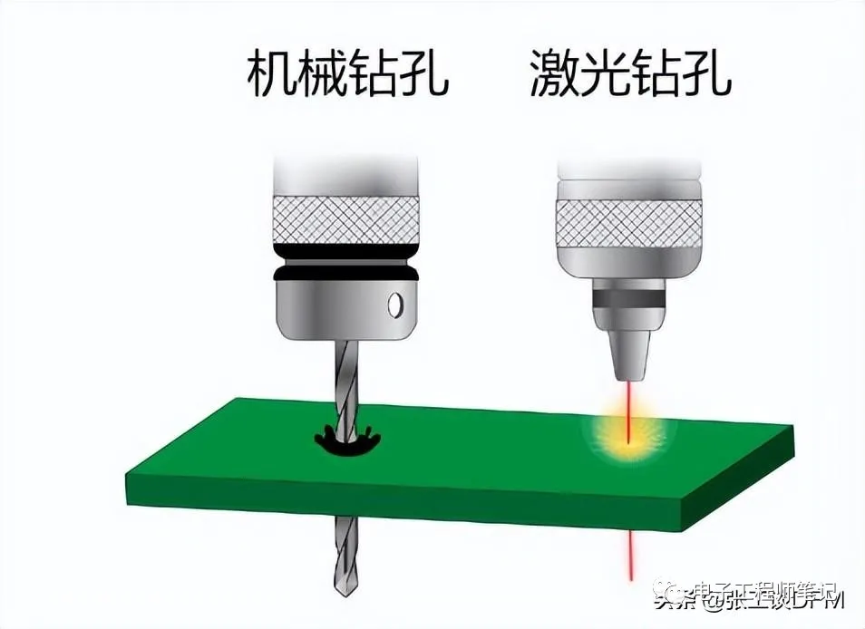
There are mainly 2 types of PCB drilling techniques: mechanical drilling and laser drilling.
PCB Drilling Techniques
1. Mechanical Drilling
Mechanical drill bits have lower precision but are easy to execute. This drilling technique utilizes drill bits. The smallest hole diameter that these bits can drill is about 6 mils (0.006 inches).
Limitations of Mechanical Drilling
When used on softer materials like FR4, mechanical drills can be used for 800 impacts. For denser materials, the lifespan reduces to 200 counts. If PCB manufacturers overlook this, it can lead to incorrect holes, resulting in circuit board scrapping.
2. Laser Drilling
On the other hand, laser drilling can create smaller holes. Laser drilling is a non-contact process where the workpiece and tool do not touch each other. A laser beam is used to remove PCB material and create precise holes, allowing for effortless control of drilling depth.
Laser technology is used to easily drill through-holes with controlled depths, allowing for precise drilling of holes with a minimum diameter of 2 mils (0.002 inches).
Limitations of Laser Drilling
PCBs are made of copper, fiberglass, and resin, which have different optical properties, making it difficult for the laser beam to effectively burn through the circuit board. In the case of laser drilling, the process is also relatively costly.
2. PCB Drilling Process
For PCB engineers, if designing a circuit board, it is also essential to understand PCB manufacturing. This ensures that PCB designs are manufacturable and reliable. If manufacturing processes are considered during design, costs can be reduced, and products can be delivered on time.
PCB Drilling Process
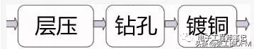
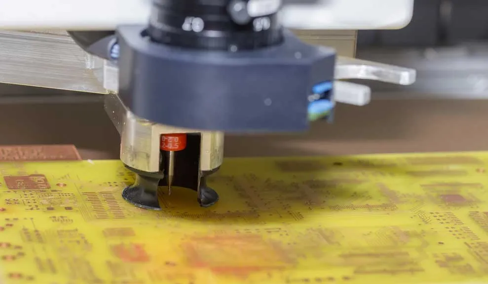
After the lamination process, the laminated board is loaded onto the exit material panel of the drilling machine. The exit material reduces the formation of burrs. Burrs are protruding copper parts formed when the drill shaft penetrates the board. On top of this panel, more stacks are loaded and carefully aligned. Finally, a sheet of aluminum foil is placed over the entire stack. The aluminum foil prevents entrance burrs and dissipates the heat generated by the rapidly rotating drill bit. Once the required number of holes are drilled, the circuit board is sent for deburring and cleaning.
Since the quality of drilling is a critical aspect, the geometry of the tools must be considered. High-speed steel (HSS) and tungsten carbide (WC) are common drill bit materials for composite material drilling. During the processing of glass fiber-reinforced polymers (GFRP), carbide tools provide longer tool life. Carbide drill bits are typically used for PCB drilling.
1. Point Angle and Helix Angle
The point angle of PCB drill bits is 130°, and the helix angle is between 30° and 35°. The point angle is measured between the most prominent cutting edges at the tip of the drill bit.
The helix angle is the angle between the side of the drill bit at the intersection.
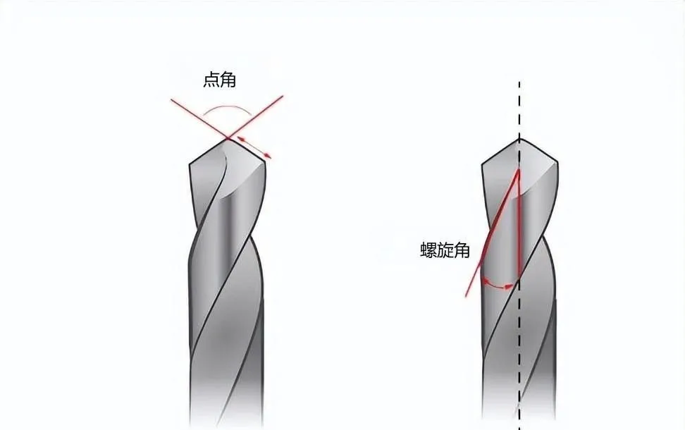
Comparison of Point Angle and Helix Angle
2. CNC Drilling Machine

Drilling Machine
A drilling machine is a pre-programmed computer numerical control (CNC) machine. Drilling is based on the XY coordinates inputted into the CNC system. The spindle rotates at high RPM, ensuring accurate drilling on the board. When the spindle rotates at high speed, heat is generated due to friction between the hole wall and the spindle, melting the resin components on the hole wall and causing resin contamination. Once the required holes are drilled, the exit and entrance panels are discarded. This is a small point of what happens in the workshop.
Unlike etching and plating processes, the drilling process does not have a fixed duration. The drilling time in the workshop varies based on the quantity of holes to be drilled.
3. Two Important Aspects of PCB Drilling
1. Aspect Ratio
The aspect ratio is the ability to effectively plate copper inside the hole (through-hole). As the diameter decreases and the depth increases, plating copper inside the hole becomes a cumbersome task. This requires a plating bath with high uniform plating capability so that the liquid can penetrate into the tiny holes.
Aspect Ratio (AR) = (Hole Depth / Drill Diameter)
The aspect ratio of through-holes is 10:1, while the aspect ratio of micro-holes is 0.75:1.
Typically, for a 62 ml PCB, the minimum drill size can be 6 mils.
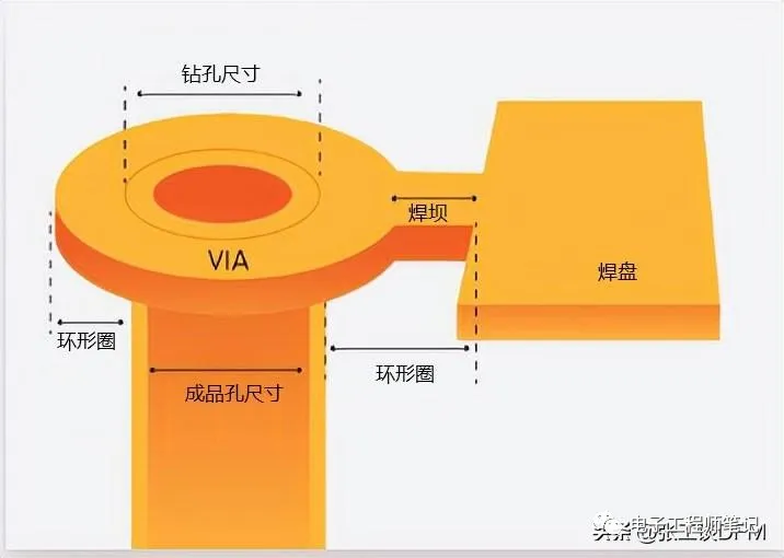
2. Drill-to-Copper Gap
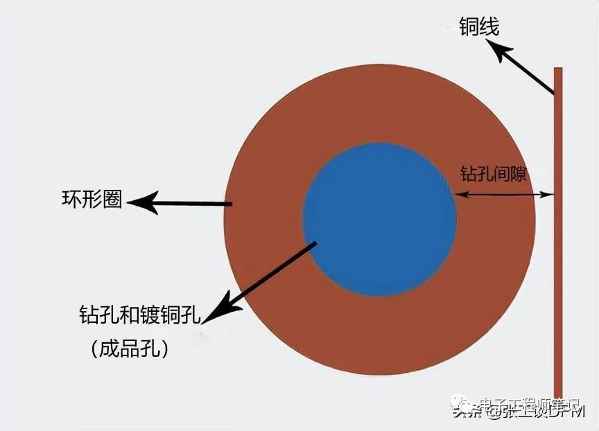
Drill-to-Copper Gap
The drill-to-copper gap is the planar gap between the edge of the hole and the nearest copper feature. The nearest copper feature can be a copper trace or any other active copper area. This is a decisive factor, as even small deviations can lead to circuit interruptions. The typical copper drill value is about 8 mils.
Minimum Gap = Ring Width + Solder Mask Dam Gap
4. Classification of PCB Drilling
Plated through holes (PTH) are conductive through-holes that carry signals and establish interconnections between different layers of the circuit board, used to secure components during PCB assembly. Non-plated through holes (NPTH) are non-conductive. These holes do not have tolerance levels, as if the hole size is too small or too large, components will not fit.
Drilling holes in a circuit board is not easy, requiring high precision and adherence to certain design rules.
PCB Drilling
1. Plated Through Hole (PTH)
Finished Hole Size (Minimum) = 0.006
Ring Size (Minimum) = 0.004
Edge-to-Edge Gap (from any other surface element) (Minimum) = 0.009”
2. Non-Plated Through Hole (NPTH)
Finished Hole Size (Minimum) = 0.006″
Edge-to-Edge Gap (from any other surface element) (Minimum) = 0.005
5. Hazards of PCB Drilling
After repeated use, drill tools can easily wear out and break. This can lead to the following issues:
1. Accuracy of Hole Position is Affected
When the drill bit fails to hit the preferred point and moves along the same axis, accuracy is compromised. Offsets in drilling can lead to hole rings becoming tangential or breaking.
2. Roughness Inside the Hole
Roughness can lead to uneven copper plating, resulting in pinholes and barrel cracks. Due to the copper plating solution penetrating the hole wall, it can also lead to reduced insulation resistance.
3. Resin Smearing
Due to the heat generated during drilling, resin in the circuit board can melt. Resin adheres to the hole walls, known as resin smearing. This again leads to poor copper plating and conductive failures between through-holes and the inner layers of the circuit.
4. Presence of Entrance and Exit Burrs
Burrs are unwanted protrusions of copper that extend from the hole after drilling, mostly appearing on the top and bottom surfaces of the printed circuit board stack.
5. Nail Head
If the nail head is not appropriate, inner layer copper may bend during drilling, leading to uneven plating and conductivity issues.
6. Delamination
Partial separation of the layers of the circuit board is considered delamination, which can occur due to improper drilling.
Remedies
1. De-resin Process
This is a chemical process used to remove melted resin deposited on the hole walls, enhancing the conductivity through the through-holes.
2. Deburring Process
This is a mechanical process that eliminates the protruding ends (crowns) of metal (copper), known as burrs. Any leftover shoulder in the hole is removed through the deburring process, followed by a repeat cleaning process.
3. Delamination
This can be avoided by using laser drilling. As mentioned earlier, in laser drilling, the workpiece and tool do not come into contact, thus eliminating delamination.
6. PCB Drilling Tips
1. Drill Pilot Holes for Proper Drilling
The first step before performing any drilling is to drill a pilot hole. This is used to prevent the drill bit from “walking,” meaning the drill bit starts from one position and then moves unexpectedly during drilling. This can be done manually with small drill bits or using an automatic tool called a drill press.
If the pilot hole is made using a drill press, the drill bit is pulled out one by one from the tool. The number of drill bits used in this process depends on the size of the PCB to be drilled. For example, if using a 0.2 mm drill bit, one hole can pull out four. When each magnetic head is removed, this process usually leaves a small metal mark on the PCB.
2. Use Vertical PCB Drill Bits When Drilling at an Angle
When drilling at an angle, drill bits are usually sold in sets and come in different sizes. Sizes include:
Wire gauge drill bits: Used for wires with a thickness of 0.8 to 1 mm.
Small drill bits: This size is suitable for holes with thickness or diameter between 0.7 and 2 mm, including flat and round shapes.
Medium drill bits: This type is used for drilling holes with thickness or diameter ranging from 2 to 10 mm, usually including flat and round shapes.
Large drill bits: This size is used for holes of 5 mm or larger. It can be flat or round, depending on the manufacturer.
3. Use the Correct Size Drill Bit
It is crucial to ensure that the drill bit size used for the PCB is appropriate. If the drill bit is too large, it may damage the components in the drilled circuit board. Conversely, if it is too small, it will not allow wires to pass through the drilled holes.
4. Use Drill Bits with Appropriate Speed and Power
The power and speed of the drill bit determine the rate at which drilling occurs on metal. The most common options are:
High-speed drill bits: This type of drill bit can quickly and efficiently drill through metal, but if used for too long at once, it can cause issues.
High-speed steel drill bits: This type is used for larger holes and is suitable for drilling multiple not too thick PCBs.
Plated drill bits: These drill bits are used for PCB drilling and plating processes, as well as for drilling thick boards or using high-frequency air hammers.
5. Use a Drill Press
A drill press is the best choice to ensure the most accurate holes are drilled. Their drilling efficiency is at least four times that of handheld drills and typically use industry-standard drill bits.
6. Understand the Operation of the Drill Press
Drill presses vary in cost and capability, but they all work by simply applying the necessary pressure to drill through metal. The greater the pressure applied, the faster the drilling speed. There are also different types of drilling, such as “cross drilling,” “insertion drilling,” “vent holes,” and “bevel end.” The most commonly used drill press type has a vertical panel (drilling metal plates at a certain angle upwards). When using this type, ensure that the drill bit is facing upwards and the angle matches the holes on the PCB.
7. Use the Drill Press for PCB Drilling
Every stage of PCB drilling can utilize a drill press. Especially when precise drilling is needed. Although adjusting the drill press takes some time, it works well as long as it is used correctly.
8. Be Careful When Drilling
Drilling on a circuit board can be challenging without the right tools and materials. Take your time and be patient when drilling, as rushing through this process may damage the circuit board. Always ensure that the drill bit does not rotate too fast or too slow while drilling. It is also important to wear safety goggles while drilling to prevent damage to your eyesight.
9. Clean the PCB After Using the Drill Bit
After completing the PCB drilling, it is essential to clean the holes using a brush and solvent. The solvent will remove any metal shavings that may have been produced during the PCB drilling, ensuring that the circuit board is ready for use after completion.
10. Apply Solder on the Drilled Holes
After completing the PCB drilling, you must apply solder to the new holes and use a soldering iron with a small tip to melt them. To ensure proper adhesion of the solder, pass a wire through one of the holes and heat it. This will prevent the solder from dripping out of the hole. Then gently press it to ensure it is securely connected.
Having the right drill bits ensures that there are no small debris and chips when drilling or slotting on the PCB. If any chips or debris are found on the drill bit, it may cause issues in the drilling process and yield undesirable results.
In PCB drilling, if done correctly, it can be completed without damaging the drill bit. If mechanical parts come into contact with the drill bit while the machine is working, they may be damaged.
7. DFM PCB Drilling Verification Techniques
1. The aspect ratio must be kept to a minimum to avoid drill bit wear.
2. The more drill bit sizes added, the more drill bits manufacturers need to use. Conversely, if the number of different drill sizes is reduced, the drilling time will decrease.
3. Confirm the types of holes you have defined (PTH/NPTH).
4. Verify the hole dimensions between the drilling files and factory prints.
5. For closed holes smaller than 0.006 inches, they must be processed out.
6. If the drill bit and other features on the copper layer fall outside the circuit board outline, reduce the through-hole size to meet the minimum aspect ratio (A/R) requirements.
7. For plated drill hole tolerances less than +/- 0.002” and for NPTH, the drilling tolerance is +/- 0.001, showing the missing NPTH hole/groove or cut location arc manufacturing diagram in the drilling file.
9. Add solder in the drilled holes.
10. Use a drill press for precision drilling.
11. Clean the PCB after drilling.