3D Printing PCBs: A New Method for Circuit Board Manufacturing
Click on the above “Mechanical and Electronic Engineering Technology” to follow us3D printing technology is revolutionizing the way we manufacture circuit boards. The traditional PCB manufacturing process involves multiple steps such as etching, drilling, and laminating, while 3D printing offers a more direct method. With 3D printing, designers can print circuit boards directly from design files, significantly shortening the time from concept to prototype.
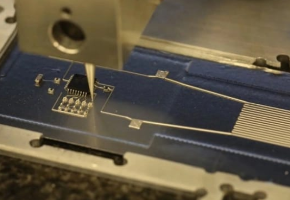
3D printing PCB technology offers many advantages. Firstly, it can quickly produce functional circuit boards, and for certain applications, even a regular desktop FDM 3D printer with conductive filament can be used for manufacturing. Secondly, 3D printing provides greater design freedom, allowing for the creation of circuits that are far more complex than traditional rectangular boards, including flexible boards, honeycomb structures, and even fully three-dimensional boards.
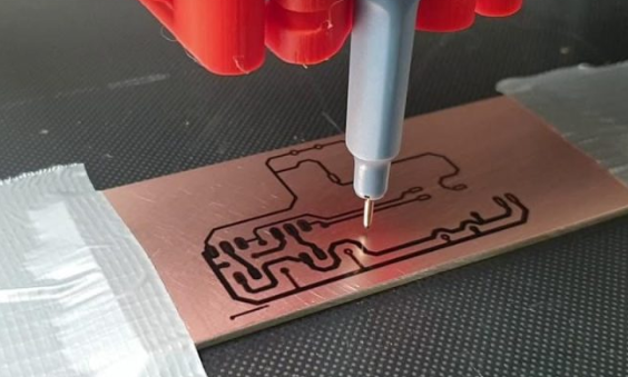
Additionally, 3D printing PCBs are cost-effective as they reduce material waste and eliminate shipping and outsourcing costs. The production speed is also faster; compared to traditional methods, 3D printed PCBs can be produced in a matter of hours. Moreover, 3D printing allows for on-demand production, reducing inventory costs and the risk of supply chain disruptions.There are primarily two methods for 3D printing PCBs. The first method involves directly printing circuits using conductive materials. This method can use inks or filaments infused with conductive particles such as silver, copper, or graphite. The second method involves printing circuit boards with hollow channels or grooves, which are then filled with conductive materials. This method can create PCBs using almost any sufficiently precise 3D printer, making it lower in cost, but may require additional steps to fill in the conductive materials.
3D printing PCB technology has been widely applied in various fields. For instance, in the military and aerospace sectors, 3D printed PCBs are used to manufacture complex electronic devices and antenna arrays. In the medical field, 3D printed PCBs are used to produce personalized medical devices. Furthermore, 3D printed PCBs are also well-suited for education and DIY projects as they allow for rapid prototyping and design iteration.Despite the many advantages of 3D printing PCB technology, it also faces some challenges. For example, the 3D printing process can be relatively slow, especially when it involves building board layers one layer at a time using filament. Additionally, the types of materials that can be used when printing circuit boards may be fewer than traditional methods, which could limit design choices. Furthermore, the circuits printed may not be as precise as those made with traditional methods, which can pose challenges for producing high-resolution patterns.The technology of 3D printing PCBs is rapidly evolving, bringing new opportunities to the electronics manufacturing industry. With continuous advancements in technology, we can foresee that in the future, 3D printing PCBs will play an important role in more fields, driving innovation in electronic products and improving manufacturing efficiency. As 3D printing technology matures, we may see increases in printing speeds and the possibility of using higher quality materials, such as graphene inks, which will further expand the application range of 3D printed PCBs.