1 Industry Overview: Value Return Amid Global Restructuring
Printed Circuit Boards (PCBs), as key electronic interconnect components in electronic products, not only support the basic functions of various components in fixed circuits but also serve as the core carrier for electrical connections of electronic components, earning the title of “Mother of Electronic Products”. In 2025, China’s PCB industry will continue to maintain its dominant position in the global market, with the market size expected to reach 433.321 billion yuan (approximately 60 billion USD), accounting for over 50% of the global share. This means that one out of every two PCBs in the world is produced or designed by Chinese companies. However, behind this massive figure, a deeper transformation is occurring—the core of industry development has shifted from traditional scale expansion to technology-driven and value chain enhancement, with high-frequency, high-speed, high-density interconnect (HDI), and advanced packaging becoming the main growth engines.
From a global perspective, since 2006, mainland China has surpassed Japan to become the largest PCB production base in the world, marking a historic shift in the competitive landscape of the industry. According to Prismark data, the PCB output value in mainland China is projected to be 41.213 billion USD in 2024, accounting for 56% of the global total; the output value is expected to reach 43.734 billion USD in 2025, a year-on-year increase of 6.1%; and it is projected to reach 49.704 billion USD by 2029, with a compound annual growth rate of 3.3% from 2025 to 2029. This growth trajectory indicates that the Chinese PCB industry has entered a mature development phase and is undergoing a strategic transformation from quantitative change to qualitative change.
2 Demand Driven: AI and Computing Power Revolution Leading PCB Market Growth
2.1 Explosive Growth in AI Computing Power Demand
In the global wave of digital transformation, artificial intelligence and computing power construction are becoming the strongest driving forces in the PCB industry. The explosive growth of AI servers has imposed technical requirements on PCBs that far exceed those of traditional products, directly driving rapid market expansion. According to a report by CICC, the AI PCB market size is expected to reach 5.6 billion USD in 2025 and 10 billion USD in 2026. This forecast highlights the enormous potential and growth elasticity of the AI-related PCB market.
The technical requirements of AI servers for PCBs are reflected in three aspects: more layers, better materials, and more precise processes. Generally, AI server PCBs typically contain a multilayer structure of 20 to 28 layers, far exceeding the 12 to 16 layers of traditional servers; in terms of price, the value of PCBs used for AI servers is several times that of traditional servers, with single-unit PCB prices rising to 8,000 to 10,000 USD. This significant value increase primarily stems from the need for AI servers to process massive amounts of data in parallel, which imposes extreme requirements on the signal transmission speed, integrity, and stability of the circuit boards.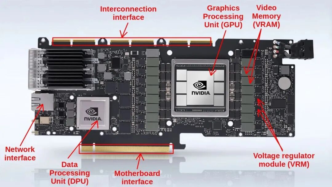
2.2 Collaborative Growth in Diverse Application Scenarios
In addition to AI servers, other application fields are also bringing diversified growth momentum to the PCB industry:
-
Smart Vehicles: The electronicization rate of vehicles has surpassed 65%, driving the proportion of automotive PCB demand from 12% in 2020 to 20% in 2025, with a market size exceeding 30 billion USD. Smart driving systems have increased the PCB usage per vehicle from 0.5 square meters in traditional cars to 3 square meters, with the PCB value for L4 autonomous vehicles exceeding 2,000 yuan. Core components of new energy vehicles, such as electronic control systems, battery management systems, and charging controllers, require a large number of high-reliability PCBs, and this trend is accelerating with increasing levels of intelligence.
-
Communication Infrastructure: The global construction of 5G base stations has exceeded 5 million, driving a 25% increase in demand for high-frequency, high-speed PCBs. The construction of low-orbit satellite constellations has generated demand for PCBs that can withstand extreme environments, with a single satellite PCB usage reaching 20 square meters, opening up a new market worth about 5 billion yuan. As communication technology evolves from 5G to 6G, the requirements for high-frequency and high-speed performance of PCBs will further increase, driving more technological iterations and product upgrades.
-
Consumer Electronics: Although growth in the traditional consumer electronics sector has slowed, the trend towards AI terminalization has injected new vitality into the consumer electronics PCB market. According to Prismark’s forecast, from 2024 to 2029, the compound annual growth rates for PCB consumption demand in the five major fields of servers/storage, consumer electronics, computers, mobile phones, and automotive electronics will reach 11.6%, 3.0%, 2.5%, 4.5%, and 4.0%, respectively. The emergence of new terminal products such as AI smartphones, AI laptops, and AR/VR devices will further drive the demand for technological upgrades in HDI boards and flexible boards.
Table: PCB Downstream Application Market Share and Growth Rate Forecast
| Application Field | 2024-2029 Compound Growth Rate | Main Driving Factors |
|---|---|---|
| Servers/Storage | 11.6% | AI computing power construction, cloud service demand |
| Consumer Electronics | 3.0% | AI terminalization, product upgrades |
| Computers | 2.5% | Commercial PC upgrades, AI PC penetration |
| Mobile Phones | 4.5% | 5G penetration, smartphone recovery |
| Automotive Electronics | 4.0% | Electrification, intelligence, connectivity |
3 Technological Evolution: Comprehensive Breakthroughs in Materials, Processes, and Architectures
3.1 Innovation in High-End Materials and Domestic Substitution
The technological competition in the PCB industry is first reflected in the materials field. Due to the skin effect, if high-speed PCBs continue to use conventional copper foil, it will lead to increasingly severe signal “distortion” as the signal transmission frequency increases. Therefore, the application of low-roughness copper foil in current high-speed materials is becoming more widespread, with materials like Mid Loss and Low Loss using reverse (RTF) copper foil as standard. To achieve high frequency and high speed in PCBs, improvements in resin, fiberglass, and overall structure are needed, or the characteristics of the substrate can be improved through wiring or other means. Thus, M9/PTFE resin, HVLP copper foil with Rz≤0.4 microns, and low-loss quartz cloth have become key materials for achieving 224G high-speed transmission.
In terms of domestic material substitution, although progress has been made in some areas, the import dependency for key materials such as high-end copper-clad laminates, special resins (like PTFE), and photoresists still exceeds 50%. Domestic substitution is accelerating; for example, the market share of Shengyi Technology’s high-frequency, high-speed copper-clad laminates has risen to 30%, with costs 15% lower than similar foreign products. Domestic manufacturers such as Nanya New Materials, Huazheng New Materials, and Shengyi Technology are also actively developing higher-end M9 and M10 grade copper-clad laminate products, with Nanya New Materials having proactively initiated the research and development of M10 grade copper-clad laminate products, with laboratory products already available. This pursuit in the materials field is narrowing the gap with international advanced levels, providing domestic PCB companies with a more resilient supply chain guarantee.
3.2 Refinement of Manufacturing Processes and Architectural Upgrades
In terms of process technology, mSAP/SAP (modified semi-additive process/semi-additive process) pushes line width/spacing below 10 microns, with laser drilling, back drilling, and high multilayer stacking processes supporting high-density interconnection. These cutting-edge processes enable PCBs to carry more components and more complex circuit designs, meeting the technical demands under high-performance computing and miniaturization trends.
Architectural innovation is also noteworthy: CoWoP packaging eliminates the ABF substrate, directly connecting chips to PCBs, which imposes high requirements on board flatness, dimensional stability, and manufacturing yield; orthogonal backplane solutions require low-loss materials such as M9 or PTFE to meet 224G SerDes transmission; embedded processes achieve heat sink elimination and system-level cost reduction by embedding power chips within the board, but require the introduction of semiconductor-grade clean rooms and IC processes. These technological breakthroughs significantly enhance PCB performance and integration, driving continuous growth in their value and accelerating deep integration with advanced packaging.
Table: Comparison of High-End and Traditional PCB Technical Specifications and Value
| Technical Parameters | Traditional Server PCB | AI Server PCB | Increase Rate |
|---|---|---|---|
| Layers | 12-16 layers | 20-28 layers | About 75% |
| Single Board Value | 1,500-2,500 USD | 8,000-10,000 USD | About 400% |
| Material Grade | Mid Loss/Regular Loss | Ultra Low Loss/Low Loss | 2-3 Grades |
| Line Width/Spacing | 20-30μm | Below 10μm | Over 50% |
| Process Requirements | Traditional Subtractive Method | mSAP/SAP | Generational Difference |
4 Restructuring the Industry Chain: Upstream Transmission and Regional Pattern Evolution
4.1 Analysis of Industry Chain Value Transmission
The upstream of the PCB industry chain includes raw materials such as copper-clad laminates, copper foil, copper balls, prepregs, gold salts, dry film, and inks; the midstream involves PCB manufacturing, which can be divided into rigid boards, flexible boards, rigid-flex boards, and packaging substrates; the downstream is widely applied in consumer electronics, servers, automotive electronics, industrial control, aerospace, medical devices, and other fields. In the cost structure of PCBs, raw materials account for about 60%, with the highest proportion being copper-clad laminates at 27.31%. The next highest are prepregs, labor costs, gold salts, copper balls, copper foil, dry film, and inks, accounting for 13.8%, 9.53%, 3.8%, 1.4%, 1.39%, 1.37%, and 1.23%, respectively.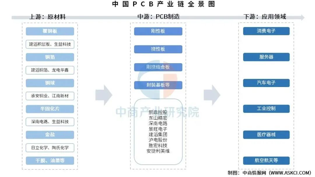
The AI computing power revolution is driving a surge in demand for high-end printed circuit boards, and its upstream key raw material, copper-clad laminates, is also encountering structural growth opportunities, with some high-end categories becoming scarce. Since the beginning of this year, international copper prices have continued to rise, reaching a peak of 11,200 USD/ton by the end of October 2025. The main reason for the high copper prices is the demand for copper consumption driven by AI computing centers, copper foil for chips, and grid upgrades. China’s new energy and power sectors maintain high prosperity, offsetting the downward drag from real estate, with low inventory amplifying price elasticity. This fluctuation in the prices of upstream raw materials is being transmitted down the industry chain, with multiple copper-clad laminate companies having raised product prices several times this year, and dynamic adjustments are still ongoing, with cost pressures and demand dividends being important drivers of price increases.
4.2 Capacity Layout and Regional Pattern
The PCB industry in China shows a clear regional agglomeration and global capacity layout trend:
-
Pearl River Delta (mainly Guangdong): centered around Shenzhen and Dongguan, focusing on high-end consumer electronics, HDI boards, and packaging substrates, accounting for about 45% of the national output value.
-
Yangtze River Delta: relying on the semiconductor industry ecosystem, focusing on automotive electronics and communication equipment, with IC substrate capacity accounting for 60% of the national total.
-
Central and Western Regions (such as Jiangxi, Hubei, Sichuan): actively undertaking capacity transfer, relying on policy dividends to develop aerospace, military, and other special PCBs, with output growth rates exceeding the national average.
To avoid trade barriers and tariffs (such as the 25% tariff imposed by the US on China), domestic companies are increasingly establishing factories in Southeast Asia (such as Vietnam and Thailand) and Mexico. Some industry companies have reduced costs by 15% or more by starting operations in Vietnam, and it is expected that by 2025, the output value of PCBs in Southeast Asia will account for 12% of the global total. This global capacity layout is not only aimed at reducing production costs but also at enhancing supply chain resilience to cope with the increasingly complex international trade environment.
5 Competitive Landscape: Layered Evolution and Diverse Paths to Breakthrough
5.1 Tier Differentiation and Market Structure
The PCB industry is highly competitive, presenting a “pyramid” structure. At the top are leading companies such as Zhen Ding Technology, Shenzhen South China Circuit, and Unimicron Technology, with annual revenues exceeding 10 billion yuan, monopolizing the high-end market through technological accumulation and global layout, with gross margins reaching 35%-40%. These companies have established solid competitive barriers in high-end fields such as AI servers, high-speed network devices, and advanced packaging, thanks to their strong R&D capabilities, leading technology levels, and quality customer resources.
Second and third-tier companies face fierce price wars in the mid-to-low-end market. These companies are usually smaller in scale, with a high degree of product homogeneity and relatively low profit margins. Against the backdrop of increasing environmental requirements and fluctuating raw material prices, the survival pressure on these companies is growing, accelerating industry consolidation. According to data, by 2025, the market share of the top ten PCB manufacturers globally will increase to 52%, a 3 percentage point increase from 2024. This indicates that market concentration is rising, and the head effect is becoming more pronounced.
5.2 Diverse Paths for Corporate Breakthroughs
In the face of intense market competition, PCB companies have adopted different breakthrough strategies:
-
Technological Breakthroughs: Leading companies focus on high-end fields, such as Shenzhen South China Circuit collaborating with Huawei to develop 6G communication PCBs, and Unimicron Technology’s 112Gbps high-speed PCBs being certified by Amazon AWS. These technological investments bring higher product added value and a more stable market position.
-
Vertical Integration: Leading companies reduce costs and enhance supply chain resilience through upstream integration. For example, Kingboard Chemical has laid out a full industry chain from “copper foil-copper-clad laminate-PCB”, reducing costs by 12%. This vertical integration model not only effectively controls costs but also ensures the stable supply of key raw materials, which is particularly valuable in the current market environment.
-
Ecological Construction and Differentiation: Some companies choose to focus on specific scenarios or customers, such as Lieban PCB binding with Huawei and Gree through a “12-layer high multilayer board + 24-hour sample delivery” model; Japan’s Kiken has developed temperature-resistant FPC for Tesla’s Cybertruck. This differentiation strategy allows companies to establish competitive advantages in specific niche markets, avoiding homogenization competition.
Table: Comparison of Strategic Layouts of Leading Companies in China’s PCB Industry
| Company Name | Core Competitive Advantage | Strategic Layout Direction | Representative Progress |
|---|---|---|---|
| Shenghong Technology | Leading in AI/HPC Field | Deeply involved in high-end AI server projects such as NVIDIA’s GB200 | Ranked first globally in AI/HPC revenue in Q1 2025 |
| Shenzhen South China Circuit | “3-In-One” Business Layout | High-end backplanes, packaging substrates | High-end backplane sample layers reach 120 layers, ABF substrates have achieved mass production below 20 layers |
| Unimicron Technology | High-Speed Network Switch Products | 800G switch and 1.6T technology | 800G switch products have achieved mass shipments, 112Gbps high-speed PCBs certified by AWS |
| Jingwang Electronics | Automotive PCBs and Multilayer PTFE Boards | AI servers, high-speed switching devices | Achieved mass production of multilayer PTFE boards, capable of supplying 800G optical module PCBs in bulk |
| Shengyi Electronics | Nearly 30 Years of Experience in Data Communication | Servers, communication equipment | Server product orders have increased to 48.96% |
6 Challenges and Risks: Constraints to Upward Breakthroughs
As the Chinese PCB industry strives for upward breakthroughs, it still faces numerous challenges:
-
Technological Dependence: In high-end materials (such as high-frequency, high-speed copper-clad laminates), advanced equipment (such as vertical continuous plating machines), and cutting-edge processes (such as multilayer boards with more than 20 layers), Japanese, Korean, and American companies still hold over 75% of the technological monopoly, with domestic substitution rates below 35%. This dependence on foreign technology makes domestic companies vulnerable in high-end market competition and limits their ability to share in the lucrative profits of the highest-end markets.
-
Geopolitical and Trade Friction: The US’s “manufacturing return” policy and technology blockade against China have exacerbated supply chain risks. Although companies have set up factories in Southeast Asia to avoid some tariffs, geopolitical conflicts may still impact global capacity layouts. Additionally, the EU’s Carbon Border Adjustment Mechanism (CBAM) may increase PCB export costs by 8-10%, posing a direct threat to the competitiveness of export-oriented companies.
-
Environmental and Cost Pressures: Environmental regulations are becoming increasingly stringent, with domestic wastewater treatment, production limitation policies, and fluctuating copper prices (up 12% year-on-year in 2025) continuously squeezing profit margins for companies. The environmental compliance requirements related to wastewater treatment and emissions during PCB production are constantly increasing, with wastewater treatment costs accounting for 3%-5% of total costs, creating significant pressure for small and medium-sized enterprises that already have low profits.
7 Future Outlook: Three Major Trends of High-End, Green, and Intelligent Development
7.1 Irreversible Trend Towards High-End Development
Looking ahead, the Chinese PCB industry will continue to break through along the high-end path. Technology will continue to evolve towards higher density, higher speed, and more advanced packaging. It is expected that by 2030, the market size of China’s PCBs will exceed 400 billion yuan, with the high-end sector growing at an annual rate of over 10%. The proportion of high-end products such as HDI and packaging substrates will continue to increase, and applications will further expand into cutting-edge fields such as 6G communication and low-altitude economy.
In the future, AI is expected to continuously iterate the technological path of PCB processes, manifested in structural integration (CoWoP, substrate integration), functional upgrades (orthogonal backplanes replacing copper connections), and material breakthroughs (M9, PTFE, quartz cloth, etc.). These technological evolutions will further enhance the value content of high-end PCBs and open up greater growth space for leading companies with technological reserves.
7.2 Green Development as an Imperative
Environmental compliance is no longer a cost burden but a core competitive advantage. “Zero-carbon transformation” will become an industry consensus, with photovoltaic factories, recycling technologies (such as recycled copper), and easily disassembled recyclable PCB designs becoming mainstream trends. Currently, the coverage of lead-free processes has increased from 80% to 95%, with photovoltaic PCB factories accounting for over 20%, and energy consumption per unit of output decreasing by 18%. Wastewater treatment costs account for 3%-5% of total costs, and advanced ion exchange membrane technology can achieve 90% copper ion recovery. The promotion and application of these green manufacturing technologies can not only reduce environmental compliance risks but also generate economic benefits through resource recycling, achieving a win-win for the environment and business.
7.3 Intelligent Empowerment for Industry Upgrades
Artificial intelligence and digital technologies will deeply empower the entire process of design, manufacturing, and testing. AI-assisted design (AI-EDA), digital twins, and 3D printing technologies will significantly shorten R&D cycles, achieve highly customized production, and continue to improve production efficiency and yield. According to a report by CITIC Securities, under this background, the planned output value growth of high multilayer boards, high-density interconnect boards (HDI boards), and IC substrates is relatively rapid, with domestic leading PCB companies expected to invest 41.9 billion yuan in projects from 2025 to 2026.
The demand for PCBs in AI servers is higher in terms of quantity, density, and performance, corresponding to increased precision requirements for related equipment, accelerated wear, and benefiting the processes of exposure, drilling, plating, and testing. Domestic PCB equipment manufacturers are expected to seize the favorable window period for AI PCBs, accelerate the validation of emerging technologies, actively undertake incremental demand, and achieve an expansion of domestic market share and value. This intelligent empowerment is not only occurring in upstream equipment but will also permeate the entire PCB production process, driving overall industry upgrades.
8 Conclusion: Strategic Transformation from Scale Expansion to Value Leap
In 2025, the Chinese PCB industry is at a critical juncture of transitioning from scale expansion to value leap. Although facing multiple challenges such as technological dependence, geopolitical issues, and cost pressures, the continuous emergence of opportunities through technological innovation, industry chain collaboration, and green sustainable development suggests that the Chinese PCB industry is expected to achieve high-quality development in the future and move towards the global high-end market.
The logic of industry growth has shifted from past demand proliferation to technology-driven, with innovative applications such as AI computing power, smart vehicles, and advanced communications driving the PCB industry into a new growth cycle. In this process, leading companies are continuously enhancing product added value and market share through technological breakthroughs, vertical integration, and differentiation strategies, while small and medium-sized enterprises are finding their survival and development space by focusing on niche markets and specialized processes.
For investors, the investment logic in the PCB industry has also undergone profound changes—shifting focus from capacity expansion and cost advantages to greater attention on companies’ technological reserves, customer structures, and influence in high-end markets. With the continuous penetration of innovative applications such as AI, new energy vehicles, and 5G/6G communications, the PCB industry, especially in high-end segments, possesses significant long-term investment value. The Chinese PCB industry is expected to transform from a “manufacturing power” to a “manufacturing stronghold” in the next five years, occupying a more important position in the global high-end market.