
Selected from TI Wireless Connectivity Forum, original post link at the bottom “Read Original”
0 Introduction
In recent years, wireless sensor network technology has developed rapidly. Due to the free and open characteristics of the 2.4 GHz communication band, various communication protocols based on this band, such as Wi-Fi and Bluetooth, have matured and been widely used. ZigBee is a low-power personal area network protocol based on the IEEE802.15.4 standard, which operates in the 2.4 GHz band. It is a low-cost, low-power, short-range wireless networking communication technology that has been widely used in various RF communication fields, such as regional positioning, line-of-sight data transmission, IoT tags, and automotive wireless electronic devices.
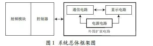
1 Overall System Framework
The system is divided into two parts: the first part is the controller and RF module, and the second part is the peripheral expansion circuit. The specific system framework diagram is shown in Figure 1.
2 Controller and RF Module Design Scheme
The main control circuit is the core of the entire system, responsible for the overall scheduling and control of the node. Considering the convenience of device operation and maintenance and the integration of the system, the main control circuit not only has data processing capabilities but also can store a certain amount of data. This design uses the ZigBee-based RF chip CC2430 as the core. This device integrates a 51-core MCU controller and RF transceiver, so the controller module and RF module are designed as a whole. Additionally, it has FLASH memory on-chip, which facilitates data storage. This device is compact, stable in performance, fast in computation, and has good scalability, meeting various needs of this design.
2.1 CC2430 Controller Circuit Configuration
In this design, the main control unit is responsible for peripheral device expansion and control, A/D conversion, data transmission, and other functions. CC2430 is a highly integrated SOC system, and its I/O port design is compact and has multiplexing capabilities. Therefore, in the design, it is necessary to save I/O port usage as much as possible, and it can be expanded when necessary. Meanwhile, the design should also have online downloading and debugging functions to meet engineering application needs.
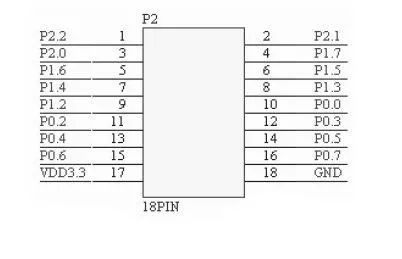
2.1.1 I/O Port Configuration
CC2430 has 21 digital I/O pins, namely P0, P1, and P2. They are all 8-bit I/O ports. Each port can be individually set as a general I/O or external device I/O. Except for two high output ports P1_0 and P1_1, the rest are used for output. The relevant I/O ports in this design are reserved in the form of connectors for easy use and expansion in different scenarios, as shown in Figure 2.
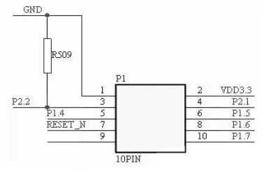
2.1.2 Debugging Interface
This design of CC2430 has online debugging and downloading functions, which can be freely configured as needed. Figure 3 shows the CC2430 debugging interface diagram, which consists of the debugging clock and data signal pins P2.2 and P2.1.
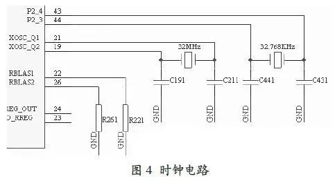
2.2 Clock and Reset
The crystal oscillator of CC2430 adopts a two-level design, one is 32 MHz, and the other is 32.768 kHz. In the CC2430 operating mode (PM0), both crystal oscillators need to work together; while in PM1 and PM2 power modes (power-saving modes), only the 32.768 kHz oscillator works; in PM3 mode, both are turned off. Meanwhile, a 1% precision resistor must be externally connected to RBIAS1 and RBIAS2 (pins 22 and 26) to provide precise bias current for the 32 MHz crystal oscillator, as shown in the specific circuit in Figure 4.
CC2430 has a power-on reset function, and manual reset can also be used. Simply pull the RESETn pin (pin 10) low to complete the reset.
2.3 CC2430 RF Module
The design of the CC2430 RF module is shown in Figure 5. In this design, in addition to the reserved external crystal oscillator for pins P2_3 and P2_4, all pins from P0_0 to P2_2 are brought out as interfaces.
The RF input and output use high-impedance differential, with pins RF_n and RF_p respectively.
This design uses a monopole antenna. To achieve the best communication performance, an unbalanced transformer should be used to achieve impedance matching.
As shown in Figure 5, discrete components L321, L331, L341, and C341 form an unbalanced transformer to connect the differential output and the monopole antenna. Since the antenna is some distance from the RF pins, it is necessary to design impedance matching for the feedback transmission line from the antenna to the RF pins. Because it is a monopole antenna, the matching impedance is 50 Ω, which is composed of the unbalanced transformer and PCB microstrip transmission line. λ is the microwave wavelength on the PCB transmission line, and the microstrip transmission line is actually λ/2 impedance matching.
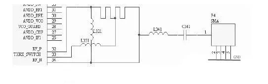
TXRX_SWITCH is an analog power output pin that can provide calibration voltage for the low-noise amplifier (LNA) and power amplifier (PA) inside CC2430. This pin must be connected to the RF_n and RF_p pins via an external DC circuit. When CC2430 is in receiving state, TXRX_SWITCH is internally grounded to provide bias voltage for LNA, and a low level can be obtained on the pin; when the chip is in transmitting state, TXRX_SWITCH supplies power voltage internally to provide bias voltage for PA, and a high level can be measured on the pin. In addition, the external antenna of this circuit uses an SMA interface.