
With the trend of the Internet of Things, wireless communication modules have become an indispensable part of various electronic devices, and the communication quality of the modules largely depends on the rationality of the antenna design. This article introduces how to choose the appropriate antenna and maximize its performance.
Reference for this article: http://www.21ic.com/app/rf/201803/755820.htm
With the advancement of technology, many manufacturers have launched various ready-made antennas to save R&D cycles. However, if engineers choose incorrectly, it may not only fail to achieve the desired effect but also waste a lot of time and costs on troubleshooting and debugging, which is counterproductive. This article will introduce several commonly used antennas and provide design suggestions based on practical experience in engineering for your reference.
Next, we will introduce the common types of antennas:
(1) Onboard PCB Antenna: Made by PCB etching, it is low-cost but has limited performance, good tunability, and can be used in large quantities for Bluetooth and WiFi wireless communication modules.
(2) SMT Patch Antenna: Commonly used ceramic antennas occupy little space, have high integration, are easy to replace, and are suitable for products with small space requirements, but this type of antenna is slightly more expensive and has a narrower bandwidth.
(3) External Rod Antenna: Good performance, no debugging required, easy to replace, high gain, suitable for various terminal devices.
(4) FPC Antenna: Connected via a feed line, flexible installation, high gain, can usually be adhered to non-metallic shells with adhesive, suitable for products with high performance requirements and ample shell space.
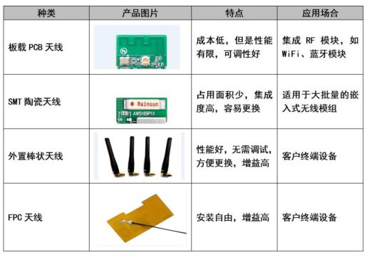
Figure 1 Common Antennas
The function of the antenna is to radiate RF signals into free space, and choosing the appropriate antenna has a significant impact on transmission distance. Antennas are very sensitive to their surrounding environment, and in many cases, even if the appropriate antenna is chosen, the expected effect may not be achieved. Since some customers are unclear about the factors that need to be considered in antenna design, we provide some practical engineering experience to help customers better design their circuits and PCBs, increasing the chances of project success.
1. Matching Circuit Design
When designing the schematic, a π network should be reserved between the antenna and the module’s RF output pin. The impedance of the antenna is affected by factors such as PCB ground, antenna installation, and surrounding metals. This network is reserved to match the antenna to 50 ohms when it deviates significantly from the standard 50 ohm impedance.
X1, X2, and X3 are reactive components. If the antenna has a standard 50 ohm impedance, X2 and X3 can remain unconnected, while X1 connects to a 220PF capacitor or a 0-ohm resistor. In the PCB design, these three components should be as close as possible to the module’s RF output pin, and the connecting transmission line should be short and straight. No ground should be laid within a 1.5mm area around the matching components to reduce the impact of parasitic parameters on the matching circuit.
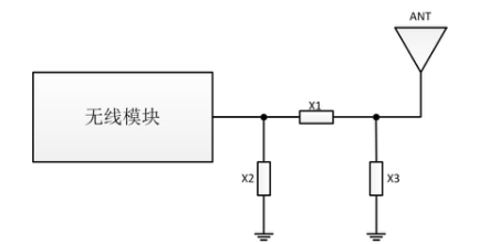
Figure 2 Matching Circuit
2. Microstrip Line Design
In PCB design, since most antennas and module output impedances are 50 ohms, to minimize energy reflection during transmission, the PCB trace from the RF output pin to the antenna should be a 50-ohm microstrip line. The commonly used substrate is FR4 (dielectric constant 4.2-4.6). Based on experience, when the line width is approximately 2.2 times the distance from the microstrip line to the reference layer, the characteristic impedance of the microstrip line is about 50 ohms. During specific design, it is recommended to use microstrip impedance control tools (like ADS, txline, etc.) for calculations and complete the microstrip line design through practical debugging. As shown in the figure below, the ground plane beneath the microstrip line must be complete, and more grounding vias should be added on both sides of the microstrip line.
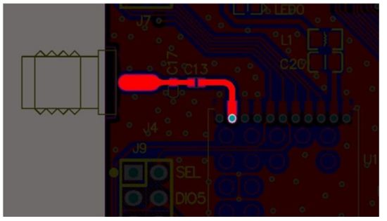
Figure 3 Microstrip Line
3. The Influence of Metal on Antennas
If there are metallic objects near the antenna, the metal can reflect electromagnetic waves, which not only affects the actual usable space of the antenna, increases the antenna’s loss resistance, and reduces radiation efficiency but also deteriorates the antenna’s radiation performance. When installing the antenna, pay attention to:
a: The antenna should be at least 5mm away from the battery;
b: The antenna should be at least 4mm away from the shielding shell;
c: In cases where an outer shell is required, do not use metallic paints or coatings on the outer shell surface.
This article is transferred from the Internet, copyright belongs to the original author. If you find it unsatisfactory, please contact us for deletion!
Advertisement
About Lichuang Mall
Lichuang Mall (WWW.SZLCSC.COM) was established in 2011, dedicated to providing customers with one-stop online procurement services for electronic components, with transaction volume leading the nation. It has a modern component warehouse of over 10,000 square meters, with over 100,000 types of stock inventory. The group’s electronic full industry chain self-operated services include: online EDA (LCEDA) + industry-leading PCB prototyping/small batch + component mall + stencil manufacturing + SMT patch + electronic design education and solutions. As a vertical mall with a complete variety of products, self-operated inventory, and guaranteed quality, all components in Lichuang Mall are sourced from original manufacturers or authorized distributors, ensuring genuine products and providing you with professional one-stop component procurement services.