Click the blue text to follow us
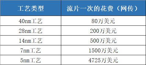
In the NHK documentary “The Story of the Electronic Nation,” a senior engineer mentioned: “During the two to three months leading up to each chip tapeout, I was filled with anxiety and couldn’t sleep. I constantly worried about what might go wrong… When the chip finally arrived and I pressed RESET for the first time, my heart raced to the extreme. The moment I released RESET was the moment that separated heaven from hell.”It is well-known that chip development is an extremely expensive endeavor, and everyone is familiar with the concept of tape-out. Tape-out refers to the process of manufacturing chips through a series of steps, similar to an assembly line. In simple terms, a chip company hands over its design to a wafer fabrication plant to produce a small number of samples, test whether the designed chip works, and based on the test results, decide whether to optimize or go into mass production. Conducting a tape-out is essential to verify the success of integrated circuit design, which is a significant reason why chip design companies often incur substantial initial costs.However, tape-out is a very costly process. No company can withstand the turmoil of a failed tape-out. Multiple failures can potentially collapse a company. Dong Mingzhu’s Gree once claimed to invest hundreds of billions in chip development, but there have been no updates since. In 2019, it was reported that Xiaomi’s Pinecone Electronics faced five consecutive tape-out failures with its Pangu S2 series chips, resulting in a painful restructuring of the design team. Some netizens humorously commented, “One tape-out is equivalent to a large flat in Shanghai,” and even released the costs of tape-outs for different process types.
Why Is Tape-Out So Expensive?
Why is the cost of tape-out so high? This leads us to the principles of chip manufacturing. Chip manufacturing involves placing hundreds of millions of transistors in a chip the size of a fingernail, with manufacturing processes reaching the nanometer scale, which can only be accomplished through photolithography. Photolithography uses light to produce the desired patterns, requiring a mask (also known as a photomask) that engraves the designed circuit diagram onto it, allowing light to pass through and imprint the pattern onto the wafer. The raw materials for this mask are inexpensive, but the machines that manufacture them are extremely costly, making the resulting masks very expensive.The mask is a tool or template for graphic transfer in the microelectronics manufacturing process, functioning similarly to a traditional camera’s “film.” Based on the required graphics, the photolithography process engraves micron-level and nano-level fine patterns onto the mask substrate, serving as a carrier for graphic design and process technology.This process of transferring the graphics from the mask to the wafer is somewhat akin to the workflow of a banknote printing machine. Imagine the photolithography machine as a banknote printer, the wafer as the banknote paper, and the mask as the printing plate. The process of printing the banknote template’s graphics onto the paper is like how the photolithography machine prints the chip graphics from the mask onto the wafer.The cost of the mask mainly depends on the chosen “process node” for the chip. The higher the process node, the more expensive the tape-out cost. This is because more advanced process nodes require more layers of masks. According to IBS data, the mask cost for 16/14nm processes is around $5 million, while at 7nm, the mask cost rapidly rises to $15 million.The overall cost of the mask includes the costs of quartz, photoresist, and other raw materials, the usage costs of Mask Writers and Inspection machines, and the generation of mask-related data, including software licenses for OPC, MDP, server usage, and labor development costs, etc. For a single chip, masks can easily require dozens of layers, necessitating numerous steps, equipment, software, and personnel, making costs naturally high.Industry insiders reveal that the mask cost for a 40nm tape-out at a foundry is approximately $600,000 to $900,000; once in mass production, each wafer may cost around $3,000 to $4,000. Therefore, when producing 5-25 wafers for product validation, the mask cost is the main expense; if mass production is high, the mask cost becomes minimal when distributed across each wafer, leaving wafer costs as the dominant expense. To be accurate, the cost averaged across each chip becomes cheaper, rather than the total tape-out cost becoming cheaper.

If you have tape-out needs, please scan the code for consultation
How to Reduce Tape-Out Costs
So, in the face of high tape-out prices, is there any way to reduce costs?MPW (Multi Project Wafer) is a tape-out method that can help design companies reduce costs. MPW refers to multiple projects sharing a single wafer, where a single manufacturing process can accommodate multiple IC design tasks. Several integrated circuit designs using the same process are placed on the same wafer for tape-out, and once completed, each design can obtain several chip samples, which is sufficient for experimental testing during the prototype design phase.In simple terms, several companies or institutions jointly purchase a set of masks, and the same wafer produced will contain several types of chips. After the wafer is cut, each entity can “take home” its respective chips. The manufacturing costs for this process are shared among all participating MPW projects based on chip area, significantly reducing product development risks. The benefits brought by MPW are evident; using multi-project wafers can lower chip production costs, provide practical opportunities for designers, and promote the transformation of chip design results, greatly benefiting the training of IC design talent, the development of small and medium-sized design companies, and the development of new products.In comparison, the advantage of sharing masks is cost savings, but it may require waiting for the foundry’s schedule, which takes more time. For those companies with ample funds or tight timelines, they can utilize a full set of masks (Full-Mask) where all masks in the manufacturing process serve their designs, typically used in the mass production phase after design finalization. However, in the current context of severe capacity shortages, foundries have varying attitudes towards different customers’ product demands, competitive advantages, market prospects, and plans. They comprehensively consider factors such as order volume, stability of future orders, and market prospects for the products.In reality, for most small and medium-sized enterprises, in addition to price, there are numerous challenges in the tape-out or mass production stages, including capacity and delivery times:1. Lack of understanding of the foundry system, lacking experience in process selection and dealing with foundries;2. High entry barriers for mainstream foundries, making it difficult for new players to apply for expected processes or support, leading to high communication costs;3. Lack of systematic supply chain management capabilities, especially during the ramp-up phase of mass production, being overly optimistic about capacity, delivery times, and quality;4. In times of capacity shortages, lacking a stocking mechanism, panic ordering or placing orders after receiving orders leads to capacity not keeping up with market demand. Additionally, fluctuations in delivery times and capacity greatly increase communication costs and reduce efficiency for startups dealing with wafer foundries.To address this, small and medium-sized chip design companies can seek cooperation with third-party tape-out service platforms that have resources and experience to jointly solve supply chain challenges.
Moore Elite: Ensuring Safe Tape-Out Services for Customers
With Moore Elite’s tape-out services, we provide a complete process platform that connects with dozens of mainstream foundries, offering tape-out services across different process nodes, including MPW, full-mask, and mass production, significantly reducing customers’ business and communication costs.On the other hand, with our self-established professional tape-out FAE team, we not only provide efficient support management to partner foundries but also help small and medium-sized companies quickly receive support for their products, assist customers in selecting the optimal processes, and ensure the security of customer data.
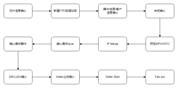
Moore Elite Tape-Out Service Reference Process
In terms of capacity, we utilize Moore Elite’s know-how to assist small and medium customers in securing capacity (including large orders, order volume trends, early queuing, timely tracking of capacity dynamics, etc.), helping customers reduce costs and shorten chip development cycles.Chip tape-out is so expensive that most developing design companies cannot afford the consequences of tape-out failures. Therefore, it is crucial to choose a reliable third-party institution to help design companies solve current supply chain challenges from technical, business, and capacity perspectives, providing optimal solutions. Chip design companies, manufacturers, and related industry service platforms and institutions should work closely together, complementing each other’s strengths, to jointly solve the “tape-out dilemma” that developers face.Since 2018, Moore Elite has upgraded its business model, investing in a 20,000 square meter self-owned packaging and testing capacity, with the Hefei Quick Packaging Engineering Center, Chongqing Quick Packaging Engineering Center, and Wuxi SiP Packaging Center sequentially put into operation. Our service capabilities focus on SiP packaging, Flip-chip packaging, rapid engineering packaging, and mass testing services based on self-owned ATE equipment. Through our integrated delivery capabilities in packaging and testing, we also provide customers with a fast track from prototype to mass production.
If you have tape-out needs, please scan the code for consultation
END
About Moore Elite

Moore Elite is on a mission to “make it easy to produce chips in China” through a one-stop chip design and supply chain platform. By combining our own packaging and testing factories with rapid response capabilities, we provide long-term, scalable, standardized, secure, and efficient “one-stop delivery from chip R&D to mass production” solutions for chip and terminal companies with diverse and customized chip needs, reducing customer risks, accelerating product launches, and improving operational efficiency, thus helping customers solve the bottleneck problem in Chinese chip production.
The company was founded in 2015, with the core team coming from IBM, SMIC, ASE, and other companies, possessing rich experience and capabilities in supply chain management. The business covers 800 chip customers, with a layout of 20,000 square meters of packaging and testing factories in Wuxi, Hefei, and Chongqing, and core equipment investments exceeding 400 million.