Before talking about FPGA, let me ask a question.
What is the essence of a chip?
I believe the essence of a chip is the circuit!
Simply put, no matter how complex a digital chip is, its foundation is just a combination of AND, OR, and NOT.
This is one of the simplest chips available on the market, the 74LS series, which is very cheap, about 20 cents;
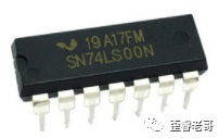
Its function is a two-input NAND gate.This is the simplest chip, and its circuit and layout are as follows.
In the above image, there are a total of 4 two-input NAND gates.
In contrast, larger chips like CPUs or GPUs have tens of millions or even over a billion gates.
However, if we delve into the lower levels of these large chips, we will find that they are also composed of AND gates, NAND gates, and other logic gates.
This is the essence of circuits; CPUs and GPUs are also forms of circuit organization.
No matter how complex a chip is, it is all described by chip design engineers using Hardware Description Languages (HDL).
It may seem like software engineers are just coding and programming, but in reality, they are building circuits.
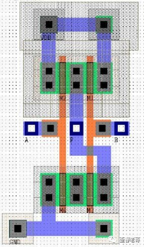
EDA tools convert this language into circuits, ultimately resulting in this layout (GDS).Then this version is submitted to manufacturers for production.The foundry converts the GDS into silicon.The packaging manufacturer completes the packaging from silicon (DIE) to chip.
This process is very similar to designing a PCB circuit.
Both involve converting circuits into PCBs for manufacturing.
The bottleneck we often talk about currently seems to be in the manufacturing stage, which is from layout to silicon.There are other issues as well, but we can discuss those in a dedicated topic later.
Today, let’s primarily discuss what the biggest problems in designing a chip are?
There are two points that are widely recognized.
First, the R&D iteration cycle is long:
It is common for large chips to take one or two years to develop. Due to functional defects or market changes, they may ultimately not be sold, necessitating a re-iteration. This is quite terrifying; small chip companies often go bankrupt due to chip failures, losing all their funds in the process.
Second, the investment in chips is high:
Chip R&D includes costs for tape-out, IP, and labor. A mask for 28nm can cost around 10 million, while 12nm approaches 25 million. Besides that, there are also costs for labor, IP, etc. Developing a 28nm chip can easily require an investment of tens of millions, while 7nm and 5nm can be hundreds of millions. Such high costs (NRE) must eventually be amortized over each chip produced.
If a project or demand only requires a few thousand or tens of thousands of units, whether it is worth developing a chip is a significant question.
If tape-out is not suitable, is there an alternative plan? A shorter iteration cycle with lower costs to meet the circuit requirements.
Here comes FPGA!
1: FPGA: The Circuit That Realizes Circuits
Field Programmable Gate Array.
Field Programmable Gate Array.
FPGA is different from dedicated chips.
As mentioned at the beginning of the article, the essence of a chip is a circuit.
So what is the essence of FPGA?
FPGA is essentially a type of chip.
However, it can also realize digital circuit functions, such as CPU, GPU, NPU, etc., all of which can be implemented internally within the FPGA, though efficiency is another matter.
Thus, the essence of FPGA is that it can realize circuits through programming.
Or rather, what kind of circuits can realize basic operations like AND, OR, and NOT?
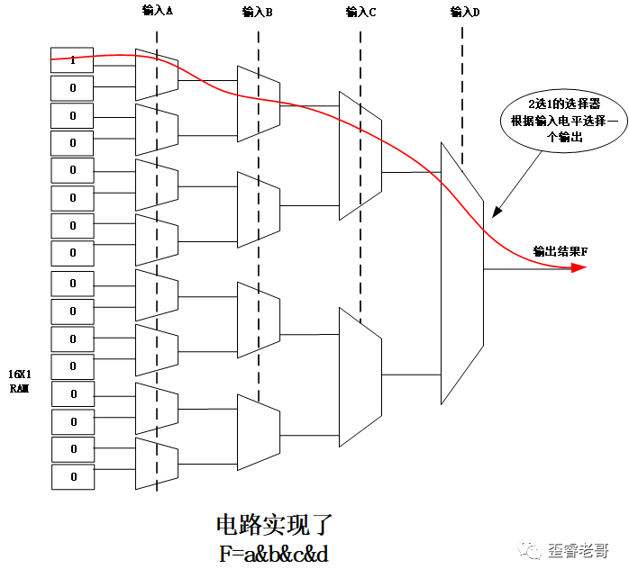
Let’s take the circuit F=A&B&C&D as an example:
A 16×1 RAM, where each bit can be programmed as 0 or 1.
This RAM has a 4-bit address, DCBA. Using these 4 bits selects the output of the RAM.
By configuring different values in RAM, we can establish the relationship between output F and inputs A, B, C, D.
In the above image, we configure the 16-bit RAM to 0000000000000001, making this circuit equivalent to F=A&B&C&D;
Only when A=B=C=D=1, F=1; in other cases, F=0;
This perfectly implements F=A&B&C&D;
Let me reiterate an important point;
When the 16-bit RAM is configured to 0000000000000001, it is equivalent to F=A&B&C&D;
Now, the string “0000000000000001” is the programming of the FPGA.
This is the most fundamental principle of FPGA;
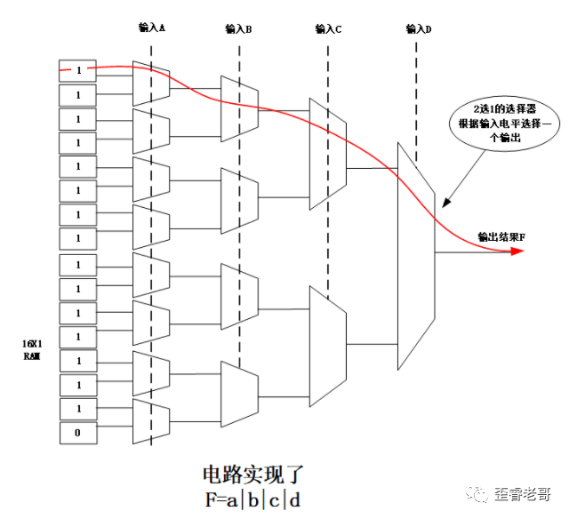
To illustrate further, how to implement the circuit F=A|B|C|D?
How is this circuit programmed:
When the 16-bit RAM is configured to 01111111111111111, it is equivalent to F=A|B|C|D.
Everyone can try: by configuring the values of the 16-bit RAM, any logical operation between A, B, C, and D can be realized.
FPGA utilizes this transformation, enabling it to describe any circuit.
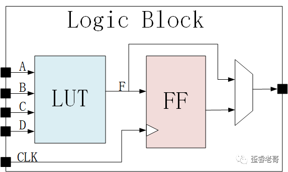
The structure shown above has a proprietary term in FPGA, called LUT, Lookup Table.
LUT constitutes the most basic unit of all FPGAs.
Since LUT can only implement digital combinational logic, a flip-flop (ff) register is added to store data;
As shown in the figure below: LUT + Register forms the basic structure of modern FPGA.
The basic structure of FPGA relies on such simple circuits to achieve incredibly complex logic.
This includes the basic structure of LUT and FF, which combine to form a basic logic unit (LOGIC BLOCK).
This LUT, which can compute inputs A, B, C, D, is called a 4-input LUT, and there are also 5-input, 6-input, and other variants.
It never strays from its essence.
This structure has not changed much since the inception of FPGA.
This circuit can also be seen as the smallest FPGA.
Currently, a chip that can implement a function has at least tens of thousands of gates and can go up to hundreds of millions.
Implementing this purely with this circuit is simply unrealistic.
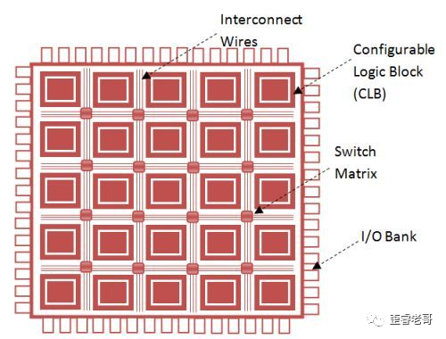
Thus, countless LUTs and FFs are needed to achieve this.
FPGA realizes an array of countless Logic Blocks (where each Logic Block consists of LUT + FF) connected by routing resources.
Combining interconnections and logic units results in an FPGA chip, as shown in the figure below.
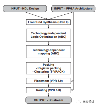
A typical FPGA development process is as follows. From HDL (Verilog hardware description language) to configuration file bitstream.
In comparison, the development process of dedicated chips goes from HDL (Verilog hardware description language) to silicon, which takes much longer.
What do these bitstreams include?
As mentioned at the beginning, when the 16-bit RAM (LUT) is configured to 0000000000000001,
it is equivalent to F=A&B&C&D;
The final generated bitstream from FPGA includes the configuration file for LUT and the configuration file for routing resources.
At this point, the design and programming of FPGA are complete.
2: EDA Tools: The Distance from Knowledge to Action
It seems that designing an FPGA chip is not complex.
The circuits are not complex, but there are not many high-performance FPGAs available in the market.
There is a huge gap between knowledge and action,
According to the principles mentioned at the beginning of this article, if a manufacturer completes the design of an FPGA chip.
When it comes time to provide it for customer use, a significant problem arises.
If an FPGA chip is provided to customers, an accompanying EDA tool must also be provided.
Without EDA tools, would you expect customers to manually generate the FPGA’s bitstream files?
The chips have been produced, but the EDA tools, are they really that easy?
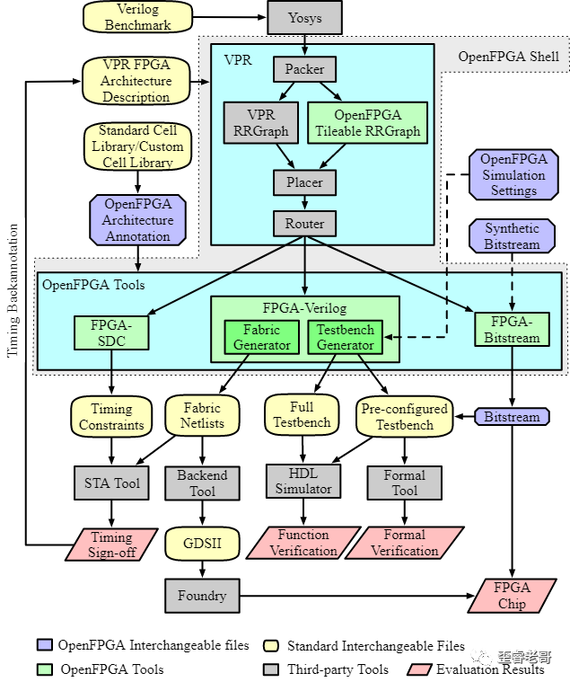
The diagram below shows an open-source FPGA design process (OpenFPGA); let’s take a look at the minimum EDA tools involved even in an open-source project.
These EDA tools needed for customers include:
6: Embedded Logic Analyzers and Debugging Tools
These are already the minimum collection, but it is much more difficult than providing a GCC compiler tool for a CPU chip.
I once installed a certain company’s EDA tools, and they were all over ten gigabytes, larger than a Windows installation disk.
If the difficulty of a CPU’s GCC tool is 1, the difficulty of FPGA’s EDA tools is between 10 and 100.
Borrowing a line from “Let the Bullets Fly”:
When the project succeeds, the chip’s contribution is only 30%.
70% is the EDA’s, and the chip only accounts for 30%.
Even this 30% still has to consider the EDA’s influence.
After working hard for a long time to produce the chip, you still have to consider the EDA tools’ influence.
Let’s see what “influence” EDA has?
Taking the layout and routing tools in the above images as an example, they seem quite complex.
If not done well, the overall utilization of the FPGA will be extremely low, and routing might not even work; you can see how important this is.
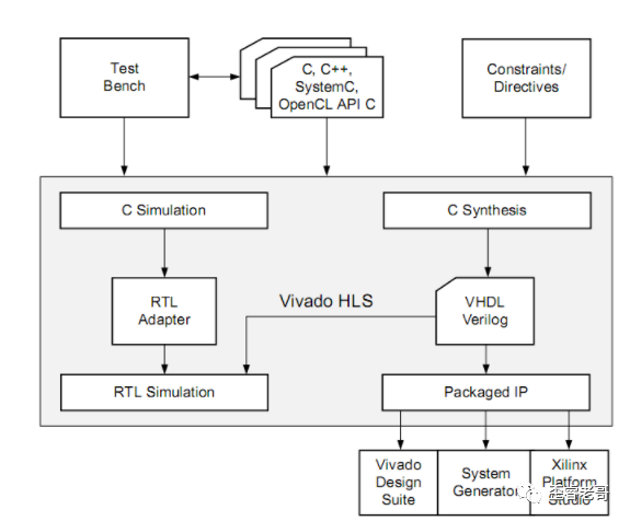
In addition to traditional EDA tools that implement HDL, like Verilog programming, there are also high-level synthesis languages like HLS.
The introduction of HLS allows software engineers to participate in FPGA design, shielding the circuit development and directly developing software, which is an additional capability of EDA tools.
However, this essentially converts high-level languages (C, C++) into hardware description languages (HDL), which are then synthesized into circuits.
The advantage is that it is closer to the habits of software engineers, but the downside is that an additional layer of conversion is added, resulting in a loss of efficiency.
3: FPGA Architecture: Fusion and Beyond
The article began by stating that FPGA consists of Logic Blocks, primarily made up of (LUT + FF), along with routing resources.
FPGA also has many hard IPs, also known as macro units.
For example, conventional IPs like PLL, SERDES, RAM, etc.
FPGA also integrates many new components.
Among these new components, a notable feature is the integration of hard CPU systems within FPGA, capable of running an OS (operating system).
CPU software programming, FPGA hardware circuit programming,
this is a combination of two swords, making it even more powerful.
Similarly, SERDES is also a necessary module for high-end FPGAs; without SERDES, the FPGA is isolated,making it impossible to achieve high-speed interconnections with other chip circuits.
Now, connections to external devices support high-speed protocols such as PCIe, SATA, and 10G/100G Ethernet.
Digital signal processing, FPGA is applied to digital signal processing and other compute-intensive tasks, such as radar, etc.
Therefore, FPGA also integrates many DSP units to perform operations like multiplication.
To share in the AI era,some FPGAs have integrated hard cores for neural network acceleration for AI processing.
To summarize, besides LUT, the hard IPs integrated within FPGA include:
1: RAM: Used for storage resources;
2: PLL: Provides high-speed clock signals and resources;
3: DSP: Multiplication operations, filters, digital signal processing modules;
4: SERDES: Achieves high-speed interfaces like PCIe, SATA, FC, and 100G Ethernet;
5: CPU System: Provides software programming development capabilities;
6: NPU Hard Core: Provides AI processing acceleration;
Depending on market needs, even more hard IPs may be added to traditional FPGAs for integration.
Integrating more functional IPs.
This is the future trend of FPGA architecture.
4: FPGA Advantages: Solving Problems Is Key
What are the differences and advantages of FPGA compared to CPU?
When discussing the merits of an architecture, the focus is on what problems it solves.
Not on whether CPU or FPGA is superior.
Only when placed in fixed application scenarios can we determine which architecture is better suited to solve these problems.
FPGA programming is circuit-based and can essentially be considered as logic gates (AND, OR, NOT) and equivalent circuits.
CPU refers to instruction operations and runs software.
FPGA operates in parallel over time, while CPUoperates serially, with a single CPU core always needing to execute instructions one by one to achieve functionality (there is also instruction-level parallelism, but the principle remains unchanged).
FPGA has a higher degree of parallelism compared to CPU’s computation methods, allowing for greater data throughput and better latency control.
However, CPUs have high frequencies, can run operating systems, and are very flexible as general computing units, which is not something FPGA can do better.
FPGA is more suitable for ASSP, used in conjunction with CPUs as dedicated computing units, ideal for processing large amounts of specific data.
Since FPGA is the “universal chip,” it seems it can replace all chip functionalities.
Is it possible to forego dedicated chip development and only use FPGA?
Compared to dedicated integrated circuits, FPGA has three disadvantages:
1: Large Area, High Cost:
Compared to dedicated integrated circuits (chips), FPGA uses LUTs to represent basic logic gate units, which roughly makes its area about ten times that of dedicated circuits, hence its cost will also be much higher.
2: Large Area, High Power Consumption:
Similarly, power consumption is not advantageous; for low-power devices, such as handheld powered devices, it is generally not feasible.
3: Low Operating Frequency, Low Computing Efficiency:
Due to longer interconnections between LUTs within FPGA, its frequency is significantly slower compared to ASICs of the same process. The delays between gates in dedicated circuits are much smaller.
However, FPGA also has clear advantages.
The greatest advantage of FPGA is its high flexibility.
Using FPGA does not require re-tapeout, saving NRE costs.
In fields such as radar, 5G, networks, storage, and high-performance computing, which involve data-intensive computations, FPGA is widely used.
Especially when demands are unclear, production volumes are small, and it is not worth making chips, or when demands are constantly changing, FPGA is a great choice.
After Intel acquired Altera, the focus of FPGA shifted to the data center market, especially with significant investments in using FPGA for acceleration in data centers. The latest Intel IPU incorporates FPGA technology to offload data center infrastructure, representing a form of DPU implementation (see the previous article: Talking about DPU — From Network to Data).
Currently, many DPU solutions utilize Intel and Xilinx FPGAs.
This reflects the changing demands for DPU in data centers.
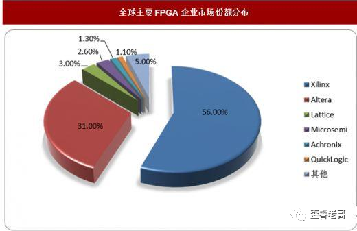
The global FPGA market was approximately 6 billion USD in 2018, with Xilinx and Altera being the most important providers in this market, while others are relatively small companies. (In 2015, Intel announced its acquisition of FPGA manufacturer Altera for 16.7 billion USD), leaving little market share for other companies.
In the past, I have used both of these FPGA brands, and they each have their strengths.
There are also many FPGA companies in China, some of which have seen reasonable shipments. Compared to foreign giants, they are still in the stage of solving the issue of availability, meeting some domestic demand. However, there is a noticeable gap in capacity, performance, and especially in EDA tools, which still requires further market refinement.
Here are two atypical cases of domestic FPGA, which are quite interesting.
In 2014, after Russia annexed Crimea, the US imposed sanctions, severely restricting Russia’s access to chips, especially high-end FPGA chips. A certain company seized this opportunity to provide FPGA chips, solving urgent needs for international friends and achieving significant profits from FPGA exports.
Additionally, a certain mobile phone manufacturer had a special transcoding format for its phone screens, meaning repairs could only be done with original screens, which were very expensive. A certain company customized a batch of ultra-small FPGAs to decode the phone screens, allowing them to use many suppliers for screens (LCD + LED, etc.), effectively replacing the original screens and performing well in the mobile phone repair market.
In these niche areas, they found their positioning and achieved significant breakthroughs in both profits and quantities.
If there are quantities of tens of thousands, hundreds of thousands, or even more, developing dedicated chips is more suitable.
If not that many, and the demands are not fixed, using FPGA is more appropriate.
In chip design, there is a step called FPGA prototyping verification, which is using FPGA to implement chip logic for equivalent testing, accelerating the iteration speed of chip design.
The article began by stating: the characteristic of FPGA is its ability to describe chip circuits.
Thus, before the tape-out of digital chips, using FPGA to load chip logic for equivalent testing is also a very important step.
From this perspective, FPGA and chips (dedicated integrated circuits) have never been opposing forces,
FPGA, the universal chip, is theoretically capable of realizing all functionalities.
However, from the perspective of PPA (Performance, Power, Area), these three dimensions are significantly limited.
FPGA is evolving, expanding into more fields to meet those changing market demands.
Some market demands have become more fixed, being replaced by dedicated chips.
The universal chip, changing applications.
Finding market positioning and solving user problems is essential for gaining a foothold.
FPGA is like this, and so is chip design.