
Some time ago, I shared the “Research Report on China’s FPGA Chip Industry (Part 1)“. Today, I will continue discussing FPGA technology.
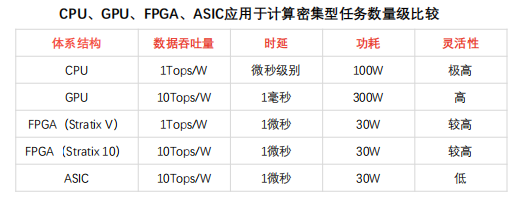
FPGAs can be used to handle various compute-intensive tasks. Relying on a pipelined parallel structure, FPGAs have a technical advantage over GPUs and CPUs in terms of latency for returning computation results.
Compute-intensive tasks: Matrix operations, machine vision, image processing, search engine ranking, asymmetric encryption, and other types of computations fall under compute-intensive tasks. These tasks can be offloaded from CPUs to FPGAs.
Performance of FPGAs in executing compute-intensive tasks:
• Computational performance compared to CPUs: For example, the Stratix series FPGAs perform integer multiplication at a level comparable to a 20-core CPU, and floating-point multiplication at a level comparable to an 8-core CPU.
• Computational performance compared to GPUs: FPGAs show an order of magnitude difference in performance for integer and floating-point multiplication compared to GPUs, but can achieve near GPU performance through configured multipliers and floating-point units.
The core advantages of FPGAs in executing compute-intensive tasks: Search engine ranking and image processing tasks have strict requirements on result return latency, necessitating reduced computation step delays. Traditional GPU acceleration solutions often involve large data packet sizes, leading to millisecond-level latency. In contrast, with FPGA acceleration solutions, PCIe latency can be reduced to the microsecond level. With future technological advances, data transmission latency between CPUs and FPGAs could be reduced to below 100 nanoseconds.
FPGAs can build an equal number of pipelines based on the number of data packet steps (pipelined parallel structure), allowing immediate output after multiple pipelines process the data packets. In GPU data parallel modes, different data units process different data packets, requiring consistent input and output from the data units. For streaming computation tasks, FPGAs have a natural advantage in terms of latency due to their pipelined parallel structure.
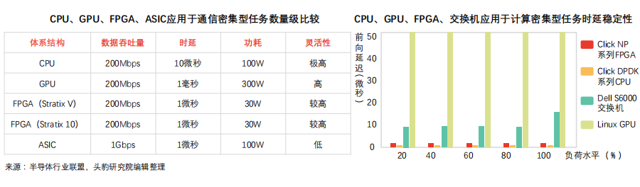
FPGAs can handle communication-intensive tasks without being limited by network cards, showing better performance than CPU solutions in terms of data packet throughput and latency stability.
Communication-intensive tasks: Symmetric encryption, firewalls, and network virtualization are examples of communication-intensive computing tasks, which are relatively less complex than compute-intensive data processing and are often limited by communication hardware devices.
FPGAs’ advantages in executing communication-intensive tasks:
① Throughput advantage: CPU solutions for communication-intensive tasks require data to be received through network cards, which can be limited by network card performance (for instance, network cards can only handle 64-byte packets at line speed, and the number of CPU and motherboard PCIe slots is limited). GPU solutions (which have high computational performance) lack network ports for processing communication-intensive task data packets, relying instead on network cards for data packet collection, which results in longer latency due to CPU and network card limitations. FPGAs can connect to 40Gbps and 100Gbps networks and process various data packets at line speed, potentially lowering the costs of network card and switch configurations.
② Latency advantage: CPU solutions collect data packets through network cards and then send computation results back to the network card. Limited by network card performance, under the DPDK packet processing framework, the latency for CPUs processing communication-intensive tasks can be nearly 5 microseconds, and CPU latency stability is weak, potentially exceeding tens of microseconds under high load, causing uncertainty in task scheduling. FPGAs can guarantee stable and extremely low latency without instructions, and FPGA solutions can be extended in complex edge devices through heterogeneous modes with CPUs.
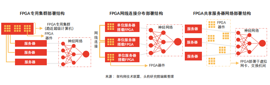
FPGA deployments include clustered and distributed models, gradually transitioning from centralized to distributed. Under different deployment methods, server communication efficiency and fault propagation effects vary.
Power burden of FPGA embedding: The impact of FPGA embedding on overall server power consumption is minimal. For example, in the FPGA-accelerated machine translation project jointly developed by Catapult and Microsoft, the overall computational capability of the acceleration module reached 103 Tops/W, comparable to the computational power of 100,000 GPUs. In contrast, embedding a single FPGA increases overall server power consumption by approximately 30W.
Characteristics and limitations of FPGA deployment methods:
① Characteristics and limitations of clustered deployment: FPGA chips form a dedicated cluster, creating a supercomputer made up of FPGA accelerator cards (for instance, the early Virtex series experimental boards deployed 6 FPGAs on the same silicon chip, with each server hosting 4 experimental boards).
• The dedicated cluster mode cannot achieve communication between FPGAs across different machines;
• Other machines in the data center must send tasks to the FPGA cluster, which can lead to network latency;
• Single-point failures can limit the overall acceleration capability of the data center.
② Network-connected distributed deployment: To ensure the homogeneity of data center servers (which ASIC solutions cannot meet), this deployment model embeds FPGAs into different servers, connecting them via a dedicated network, thus solving issues of single-point failure propagation and network latency.
• Similar to the clustered deployment model, this model does not support communication between FPGAs across different machines;
• Servers equipped with FPGA chips have highly customized characteristics, leading to higher operational and maintenance costs.
③ Shared server network deployment: In this deployment model, FPGAs are placed between network cards and switches, significantly enhancing network acceleration functions and achieving storage virtualization. FPGAs set virtual network cards for each virtual machine, moving the data plane functionality of virtual switches into the FPGA, eliminating the need for CPUs or physical network cards in the network data packet transmission process. This solution significantly enhances virtual machine network performance (25Gbps) while also reducing data transmission network latency (10 times).
In shared server network deployment models, FPGA accelerators help reduce data transmission latency, maintain stable latency in data centers, and significantly enhance virtual machine network performance.
FPGA acceleration of Bing search ranking in the shared server network deployment model: Bing search ranking in this model uses 10Gbps dedicated network cable communication, with each network group consisting of 8 FPGAs. Some are responsible for extracting signal features, some for computing feature expressions, and some for calculating document scores, ultimately forming a robot-as-a-service (RaaS) platform. Under the FPGA acceleration scheme, Bing search latency is significantly reduced, and latency stability exhibits a normal distribution. In this deployment model, remote FPGA communication latency is negligible compared to search latency.
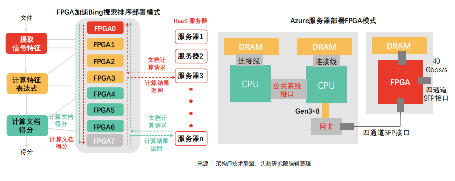
Azure server deployment FPGA model: Azure adopts the FPGA shared server network deployment model to address the high costs associated with network and storage virtualization. As network computing speeds reach 40Gbps, the costs of CPU for network and storage virtualization surge (each CPU core can only handle 100Mbps throughput). By deploying FPGAs between network cards and switches, network connections extend throughout the data center. With a lightweight transport layer, latency can be controlled within 3 microseconds for the same server rack and within 20 microseconds for all FPGA racks in the same data center.
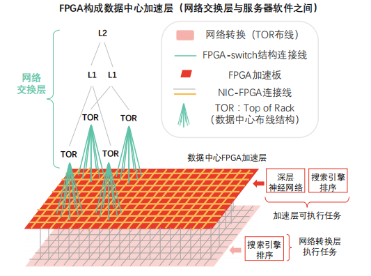
Leveraging high bandwidth and low latency advantages, FPGAs can form a data center acceleration layer between the network switching layer and server software, achieving superlinear performance improvements as the scale of distributed accelerators expands.
Data Center Acceleration Layer: FPGAs are embedded in the data center acceleration plane, situated between the network switching layer (rack layer, first layer, second layer) and traditional server software (software running on the CPU layer).
Acceleration layer advantages:
• The FPGA acceleration layer provides network acceleration and storage virtualization acceleration support for each server (providing cloud services), with remaining resources in the acceleration layer available for deep neural network (DNN) and other computational tasks.
• As the scale of FPGA accelerators expands in distributed network modes, the improvement in virtual network performance exhibits superlinear characteristics.
Principle of performance improvement in the acceleration layer: When using a single FPGA, the memory of a single chip is insufficient to support full model computation tasks, necessitating continuous access to DRAM for weights, which is limited by DRAM performance. The acceleration layer supports virtual network model single-layer or partial computation tasks through a large number of FPGAs. In this mode, the chip memory can fully load model weights, breaking through DRAM performance bottlenecks and fully leveraging FPGA computational performance. The acceleration layer must avoid excessive fragmentation of computational tasks that leads to imbalanced computation and communication.
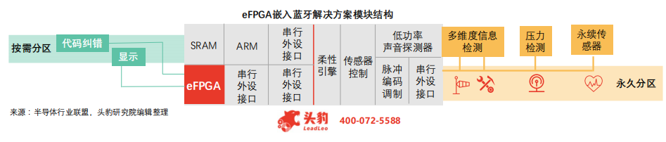
Embedded eFPGA technology outperforms traditional FPGA embedding solutions in terms of performance, cost, power consumption, and profitability, providing flexible solutions for different application scenarios and market demands.
Drivers of eFPGA technology: The rising complexity of design along with the economic trend of declining device costs has triggered market demand for eFPGA technology.
Device design complexity: The software tools related to SoC design implementation processes have become increasingly complex (for example, Imagination Technologies provides PowerVR graphics interfaces and Eclipse integrated development environments to meet customer needs for complete development solutions), leading to increased engineering time (compilation time, synthesis time, mapping time; the larger the FPGA, the longer the compilation time) and higher molding costs (the cost of FPGA chips is about 100 times that of ASIC chips of the same specifications).
Device unit functional costs continue to decline: In the late 20th century, FPGA average prices were high (over 1,000 yuan), and under traditional models, the integration of FPGA and ASIC designs led to increased ASIC chip die area and size, raising complexity and costs. In the 21st century, compared to mass-produced mixed devices, FPGAs are more often used for prototyping and pre-production design, with costs continuing to decrease relative to traditional integration (as low as about 100 yuan), allowing for flexible applications. Advantages of eFPGA technology:
Higher quality: eFPGA IP cores and other functional module SoC designs perform better than traditional FPGA embedding ASIC solutions in terms of power consumption, performance, size, and cost.
More convenient: The fast-changing demand in downstream application markets means that the reprogrammable characteristics of eFPGA help design engineers update SoCs, allowing products to maintain a longer market presence and significantly enhance profits, revenues, and profitability. Under eFPGA solutions, SoCs can operate efficiently, quickly updating to support new interface standards while rapidly integrating new functions to meet segmented market demands.
More energy-efficient: Embedding eFPGA technology in SoC designs can enhance overall performance while reducing total power consumption. By leveraging the reprogrammable features of eFPGA technology, engineers can reconfigure solutions based on hardware for specific problems, thus improving design performance and lowering power consumption.
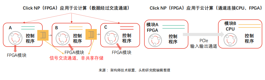
FPGA technology does not rely on instructions or shared memory, providing low-latency streaming communication capabilities in cloud computing network interconnect systems, widely meeting acceleration needs between virtual machines and processes.
FPGA cloud computing task execution flow: Mainstream data centers use FPGAs as acceleration cards for compute-intensive tasks, with Xilinx and Altera launching OpenCL-based high-level programming models, where the model relies on CPUs to reach DRAM, transferring tasks to FPGAs, notifying execution, and then FPGAs complete the computation and send results back to DRAM, which are finally transferred to CPUs.
FPGA cloud computing performance upgrade potential: Currently, communication between data center FPGAs and CPUs often uses DRAM as an intermediary, completing communication through the processes of burning DRAM, starting kernels, and reading DRAM (FPGA-DRAM data transfer speeds are relatively slower than CPU DRAM), with latencies nearing 2 milliseconds (OpenCL, shared memory among multiple kernels). There is potential for upgrading CPU-FPGA communication latency, which can be efficiently achieved through PCIe DMA, potentially reducing latencies to as low as 1 microsecond.
New communication scheduling mode for FPGA cloud computing: In the new communication mode, FPGAs and CPUs do not need to rely on shared memory structures and can achieve high-speed communication between intelligent units and host software through pipelines. Cloud computing data center tasks are relatively singular and repetitive, mainly involving virtual platform network construction and storage (communication tasks) as well as machine learning, symmetric and asymmetric encryption/decryption (computational tasks), which are more complex algorithms. Under the new scheduling mode, CPU computational tasks tend to fragment, and in the long run, cloud platform computing centers may rely primarily on FPGAs, offloading complex computation tasks to CPUs instead of the traditional model where CPUs offload tasks to FPGAs.
The global FPGA market is dominated by four major players: Xilinx, Intel (which acquired Altera), Lattice, and Microsemi, who monopolize over 9,000 patents, controlling the industry’s “air supremacy”.
Since the formation of the FPGA chip industry, over 70 companies globally have participated in competition, with new startups emerging continuously (such as Achronix Semiconductor, MathStar, etc.). Product innovation provides momentum for industry development, with new types of programmable logic devices (which have mixed signal and analog characteristics) innovating rapidly, such as Cypress Semiconductor developing programmable mixed-signal circuits PSoC (Programmable System on Chip), and Actel launching Fusion (programmable mixed-signal chips). Additionally, some startups have introduced field programmable analog arrays FPAA.
With the evolution of intelligent market demand changes, highly customized chips (SoC ASIC) face increased market risks due to large non-recurring investments and long R&D cycles. In contrast, FPGAs hold advantages in parallel computing tasks and can replace some ASICs in high-performance, multi-channel fields. The demand for multi-channel computing tasks in artificial intelligence drives FPGA technology toward mainstream adoption.
Based on the advantages of FPGA chips in small batch (with 50,000 as the boundary) and multi-channel computing dedicated devices (radar, aerospace equipment), some downstream application markets are replacing ASIC application solutions with FPGAs.
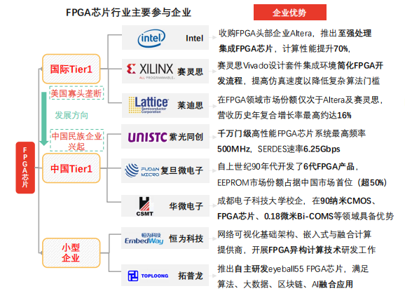
Chinese FPGA chip R&D companies include Unisoc, Guowei Electronics, Chengdu Huayi Electronics, Anlu Technology, Zhiduojing, GaoYun Semiconductor, Shanghai Fudan Microelectronics and Jingwei Qili. From a product perspective, the performance indicators of Chinese FPGA hardware are significantly behind those of Xilinx and Intel. Unisoc is currently the only company in the Chinese market capable of independently developing and manufacturing high-performance FPGAs with tens of millions of gates. Shanghai Fudan Microelectronics launched self-owned intellectual property FPGA products with hundreds of millions of gates in May 2018. Chinese FPGA companies are closely following the footsteps of major manufacturers, targeting markets such as artificial intelligence and autonomous driving, creating a complete product line across high, medium, and low-end segments.
The current breakthrough point for Chinese FPGA companies is that their chip design software and application software are not unified, leading to resource waste on the client side. Leading manufacturers can take the lead in concentrating industry chain resources to enhance the overall competitiveness of the industry.
ASIC Technology Special Analysis
2021 Overview of China’s Intelligent Network Card Industry

Disclaimer: This account focuses on sharing relevant technologies; the content and views do not represent the position of this account. All retrievable content is duly credited. If there are copyright issues with published articles, please leave a message to contact for deletion. Thank you.
E-book <Complete Knowledge of Server Basics (Ultimate Edition)> has been updated, providing in-depth explanations of knowledge points, with a complete 182-page version available for download.
How to obtain: Click “Read Original” to view the details of the PPT editable version and the PDF reading version.
Warm Reminder:
Please search for “AI_Architect” or “Scan” to follow the public account for real-time updates on in-depth technical sharing. Click “Read Original” to access more original technical resources.


Reprint Statement: Reprinting articles from this account must credit the author and source. If there are copyright issues with published articles, please leave a message for processing. Thank you.
Recommended Reading
For more architecture-related technology knowledge summaries, please refer to the “Architect Full Store Technical Materials Package” related e-books (37 books of technical materials packaged together can be obtained through “Read Original”).
All store content is continuously updated. Now order the “Complete Store Technical Materials Package (Full)”, and you can enjoy “free” updates for all store content in the future, with a price of only 198 yuan (original total price 350 yuan).
Warm Reminder:
Scan the QR code to follow the public account, click the Read Original link to obtain details about the “Architect Technical Full Store Material Package Summary (Full)” e-book materials.