The previous blog discussed SoC design, but I felt it wasn’t thorough enough. This time I’m prepared to elaborate on SoC design and clarify several core issues.
To explain SoC clearly, we need a good “textbook” or reference. Unfortunately, there isn’t a textbook that explains SoC comprehensively. I’ve read papers for many years and have probably looked at hundreds of papers related to SoC. However, most papers are either too complex or too abstract. Among all the papers I’ve read, I believe one paper is the most suitable for explaining SoC. This is the paper titled “A 60mW Baseband SoC for CMMB Receiver” published by Professor Zeng Xiaoyang’s research group at Fudan University at ASP-DAC 2012 (the project supervisor should be Associate Professor Chen Yun). This paper contains an illustration that clearly explains the basic structure and design methodology of SoC. Moreover, this paper is aimed at CMMB (the protocol for mobile digital TV promoted in China) receivers and reflects some ideas on how computer network protocols are implemented.
Professor Zeng is my wife’s doctoral advisor and one of the mentors who guided me into the field of SoC design. Over the years, he has provided me with significant help and guidance. Therefore, before discussing this paper, I need to prepare thoroughly to avoid making mistakes or presenting poorly.
So everyone can search for this paper and prepare in advance.
—
First, I declare that the images used in this article come from the paper “A 60mW Baseband SoC for CMMB Receiver”, authored by Chuan Wu, Jialin Cao, Dan Bao, Yun Chen (Associate Professor Chen Yun), and Xiaoyang Zeng (Professor Zeng Xiaoyang), with the affiliation being the National Key Laboratory of Application-Specific Integrated Circuits, Fudan University. The copyright of the images belongs to the original authors. For any technical cooperation needs, please contact the original authors directly.
Let’s start with the images!
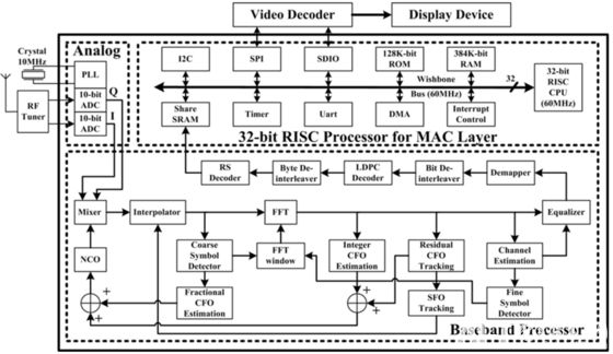
From this image, you can see clearly that it is divided into three parts. The Analog part consists of mixed-signal circuits, including two 10-bit ADCs and a PLL for generating clock signals. The two ADCs serve to convert the IQ modulation’s two signals from digital to analog. For an introduction to IQ modulation, you can refer to my blog:
http://blog.chinaaet.com/molf/p/29748
The second part is the Baseband Processor. Strictly speaking, this is not a processor; it’s just a hardware IP that implements baseband signal processing. From left to right, it includes functions such as mixing, symbol synchronization, channel estimation, equalization, demapping, and channel decoding. Friends who have studied communication theory should understand that this is the basic processing required for a digital receiver.
The third part is a 32-bit RISC Processor for the MAC Layer. This is clearly an embedded microprocessor centered around a 32-bit RISC CPU, which can also be described as a simple SoC.
That concludes the explanation, which seems rather “ordinary”. So, of course, it won’t end there. Next, we’ll take a fresh look at this image from both the SoC and computer network perspectives.
From the SoC perspective, first, note this part:

This is referred to as Share SRAM. Who shares this? It is shared between the Baseband IP and the RISC processor. Therefore, this SRAM can be considered a dual-port RAM (it may not necessarily be implemented as true dual-port RAM). One end is where the Baseband writes the data recovered after various signal processing and channel decoding. The other end is where the CPU reads this data via the on-chip bus for further processing.
Now let’s take a look at the RISC processor part.
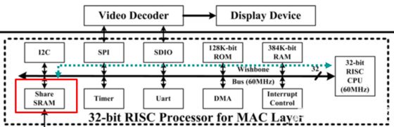
From the CPU’s perspective, this Share SRAM is no different from other ordinary on-chip SRAMs. They occupy a certain address space and can all be read and written through the bus. However, the data in this Share SRAM has specific meanings and structures. Since this is aimed at a CMMB standard receiver, the data obtained after a series of communication signal processing should conform to the CMMB standard data frames. These data frames must consist of control words for frame headers and trailers along with payload data. The CPU’s role is to parse these received data frames under the guidance of instructions and control the next actions based on the parsed results.
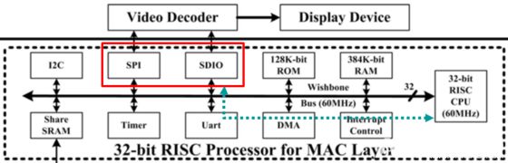
The fully parsed data will be transmitted to an external video decoder via SDIO and SPI. The video decoder will decode the data, restore it to image signals, and then display the parsed image signals on the display device, completing the entire process of receiving signals according to the CMMB protocol.
The above is the entire process of SoC operation from the SoC perspective.
However, looking at it only from the SoC perspective provides a rough overview of the entire SoC operation. To design an SoC chip, this understanding is far from sufficient. Next, we need to examine the issue from the perspective of computer network protocols.
How should we look at it from a computer network perspective? Let’s first revisit what functions this SoC serves. The function of this SoC can be simply described by the following image:
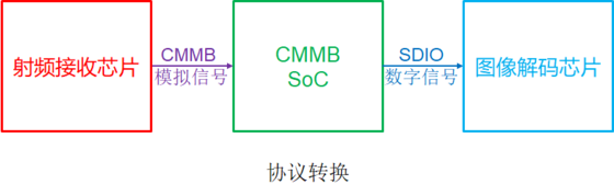
In simple terms, this SoC chip processes the analog signals received in CMMB protocol format from the RF receiving chip and converts them into SDIO protocol format to send to the image decoding chip. This process essentially implies a protocol conversion function.
How to achieve protocol conversion? This brings us to computer networks, the OSI seven-layer model, and so on.
Let’s look at an image first.
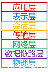
OSI seven-layer model, which I believe students who have studied a little computer networking should understand. Back in my days as a communication engineering graduate, I could recite this seven-layer model backward (of course, I could also recite it forward).
But reciting it backward means nothing if one does not understand its true meaning. What exactly does XX layer mean? Why do we need to layer it? Is this layer hardware or software? These are all unclear.
In fact, the two core concepts in computer networking are related to layering: one is peer-to-peer, and the other is service. Peer-to-peer means abstracting the communication process into interactions between peer entities. Interaction operations rely on support from lower layers, and these supports are called services.
The services provided by lower layers to upper layers need to be accessed in some way, which is called the “service access point”.
Visually, it should look like this:
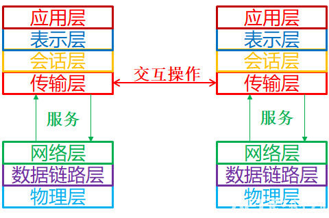
For example, when designing the transport layer, the focus is on how to interact with the transport layer of the other party. Typical functions implemented in the transport layer, such as flow control and quality of service, are coordination operations between two transport layers.
The transport layer must rely on lower layers to provide support to achieve these operations. At the very least, it must ensure proper delivery and reception of packets, so services are required. Moreover, these services must be accessed in a reasonable manner, which is the service access point.
Now, in this SoC case, where do layering, services, and service access points manifest?
Let’s return to this image:
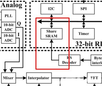
From the SoC perspective, this is the interface between the bus and the IP core, which is the channel through which the CPU reads data processed by the IP core via the bus.
From the computer networking perspective, this is the service access point. It is where the physical layer provides services to the data link layer. The data link layer, existing in software form, accesses the services of the physical layer by reading and writing to the SRAM while also controlling the physical layer through this SRAM. As for the controls implemented, there are many to detail. In brief, it can control the state of transmission and reception, which is the media access control (MAC).
This is the hardware service access point, and for software, it is even simpler. It can be abstracted as a function. Parameters are passed in, and results are read out. Because many practical protocol stacks operate at the software level, many people mistakenly believe that protocols are a special kind of software. This leads to an old professor from a certain school (I forgot which one, and even if I remembered, it wouldn’t be convenient to say) asking me if re-downloading software could turn Zigbee into Bluetooth, since they both operate in the 2.4G frequency band…
Finally, the process of sending the parsed data out via SDIO can be illustrated with this image.
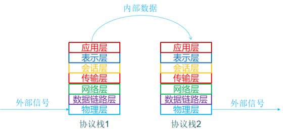
This shows the layered signals packed according to the protocol stack being parsed layer by layer, ultimately restoring them to internal data. Then, this data is recombined and reformatted according to another protocol before being sent out through the interface. This achieves a form of protocol conversion. In this SoC example, it is the conversion from CMMB to SDIO for transmission.
Of course, it is also possible not to restore the original data but to cut it in half for conversion. This would require implementing part of the CMMB protocol stack on the decoding chip. Such a design is not impossible, but it does seem a bit odd.
That’s about it for today. SoC design is a vast topic, and I hope today’s discussion gives everyone a more comprehensive understanding of SoC design. Finally, from today’s example, you can see that SoC design encompasses a wide range of topics. It is not enough to just know how to write a few lines of Verilog. It requires a series of work from application, system architecture, IP and interface design, to algorithm implementation. For those who want to research and work in this direction, you should have a clear understanding and be prepared. At the same time, weigh whether you are truly willing to invest your youth in this direction.
Next, I will fill the gap by discussing the technical aspect of “gaseous circuits” in a movie, as the film “密战” is now available for free viewing on Youku.
Everyone can watch the movie to prepare:
http://v.youku.com/v_show/id_XMzIyNzU5NTk1Mg==.html?spm=a2hww.20027244.m_250012.5~5!2~5~5~A