“IT有得聊”是机械工业出版社旗下IT专业资讯和服务平台,致力于帮助读者在广义的IT领域里,掌握更专业、更实用的知识与技能,快速提升职场竞争力。 点击蓝色微信名可快速关注我们!AI processors need to handle a large amount of parallel data, which requires a high degree of parallelism. There are various strategies for increasing the parallelism of processors, with common approaches including enhancing Instruction Level Parallelism (ILP), Data Level Parallelism (DLP), and Thread Level Parallelism (TLP). Enhancing Instruction Level Parallelism refers to increasing the number of instructions that can be executed per clock cycle, with Very Long Instruction Word (VLIW) technology and Superscalar technology being two typical methods for improving instruction-level parallelism. Enhancing Data Level Parallelism refers to increasing the amount of data that can be processed per clock cycle, with Single Instruction Multiple Data (SIMD) being a typical technique for improving data-level parallelism, and Single Instruction Multiple Thread (SIMT) being a typical technique for enhancing thread-level parallelism. Below, we will take the VLIW+SIMD architecture design as an example to introduce a typical hardware architecture implementation scheme for AI processors.
VLIW+SIMD Architecture Design
The VLIW architecture is a typical processor architecture that utilizes instruction-level parallel mechanisms. Its core idea is to issue multiple instructions to different execution units for parallel execution in each clock cycle. The instructions issued in the same clock cycle form an Instruction Package, and there should be no dependencies between the instructions in the instruction package. The parallel execution of instructions in the VLIW architecture does not require hardware dynamic scheduling, relying entirely on compiler-level instruction scheduling.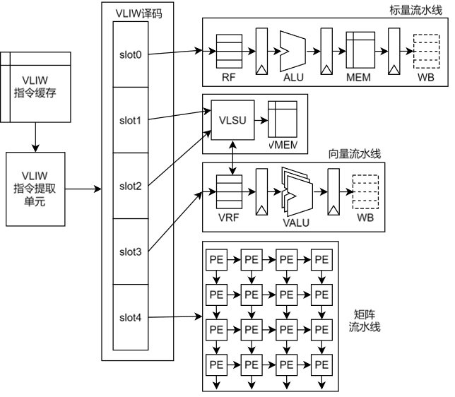
Figure 1.Example of VLIWArchitectureFigure 1 is a schematic diagram of a VLIW architecture processor, where VLIW instructions are stored in the VLIW Instruction Cache. The fetching of VLIW instructions is done in units of instruction packages, with typical widths of 64bit, 128bit, and 256bit. It can be seen that due to the wide width of the instruction package, and the fact that the compiler may not always find suitable instructions to fill the entire instruction package during the instruction packing process, there may be a large number of No Operation (NOP) instructions in the instruction package, resulting in a lower instruction density for the VLIW architecture. Therefore, the instruction cache capacity for VLIW architecture generally needs to be set relatively large.After the instructions are fetched, they are sent to the VLIW decoding unit for instruction decoding, where the instruction types in the instruction package are determined, and the instructions are sent to the corresponding execution units. The instruction package can be divided into multiple instruction slots, with each instruction slot holding one instruction. The instruction package shown in Figure 1 contains 5 instruction slots, where Slot0 is a scalar instruction sent to the scalar pipeline; Slot1 is a Vector Load instruction, and Slot2 is a Vector Store instruction, which are sent to the Vector Load Store Unit (VLSU) to complete the loading and storing of vector data; Slot3 is a vector execution instruction sent to the vector pipeline; and Slot4 is a matrix operation instruction sent to the matrix pipeline. It is important to note that the instruction type corresponding to each Slot is not completely fixed; for example, in vector computation-intensive code, the instruction package may have two Slots holding Vector Load instructions, one Slot holding a Vector Store instruction, one Slot holding vector operation instructions, and the last Slot holding other instructions; in scalar computation-intensive code, multiple Slots can hold scalar instructions. This flexible instruction packing method can improve instruction packing efficiency to some extent.The core of VLIW architecture design lies in instruction-level parallelism. As the number of slots in the instruction package increases, the complexity of instruction scheduling by the compiler also increases: when there are only two slots in the instruction package, it is relatively easy for the compiler to fill the instruction package, but when there are more slots, it becomes difficult for the compiler to find multiple unrelated instructions within a local range. Additionally, since these slots have restrictions on the types of instructions they can hold, the scheduling difficulty for the compiler increases, which may lead to multiple NOP instructions being inserted into the instruction package. Furthermore, as the number of slots in the instruction package increases, the capacity of the instruction cache also needs to be increased, and the number of execution units in the hardware must also be increased, which adds to the hardware area overhead. Therefore, the number of instruction slots in the instruction package should not be too many, typically ranging from 3 to 6.When the enhancement of instruction-level parallelism encounters bottlenecks, data-level parallelism can be increased. SIMD is a technique for enhancing data-level parallelism, where multiple channels perform the same instruction operation on different input data driven by a single instruction. The comparison between SISD (Single Instruction Single Datastream) and SIMD is shown in Figure 2. In processors designed with SISD, one instruction corresponds to one set of data, while in processors designed with SIMD, one instruction corresponds to multiple sets of data.
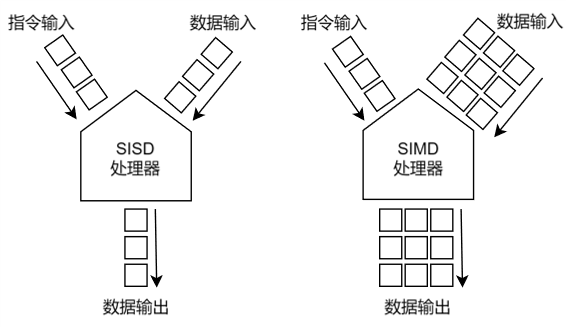
Figure 2. Comparison of SISD and SIMDSIMD technology is particularly suitable for efficiently processing large-scale, highly parallel computing scenarios, significantly reducing bus access cycles and improving data processing parallelism. However, it has high requirements for algorithms and data structures; if there are many dependencies between single points in the algorithm, it is not suitable to use this technology for acceleration. Additionally, in high-parallelism SIMD architecture processors, if the data to be processed is distributed relatively discretely, it may be necessary to perform operations such as merging, splitting, and compressing on this data, which requires a large amount of hardware resources and increases the complexity of backend layout and routing. This is similar to the bottlenecks encountered when enhancing instruction-level parallelism, so the data-level parallelism of SIMD architecture should also not be too high.The above content is excerpted from “AI Processor Hardware Architecture Design”Authors: Ren Zimu, Li Dongsheng
Recommended Reading

▊ “AI Processor Hardware Architecture Design”“
Compiled by Ren Zimu and Li Dongsheng
-
Recommended by 14 industry experts
-
The document and details restore the essence of architecture design,analyzing advanced AI processor architectures/microarchitectures and related technologies comprehensively
-
Integrating years of experience from senior engineers in developing high-performance processors, starting from the architecture design of AI processors, comparing the advantages and disadvantages of various architectures of AI processors, and detailing the architecture and microarchitecture design of each component, progressing step by step, combining text and images. Users can complete the design and verification work of AI processors from 0 to 1 based on the introduction in this book.

撰  稿  人:计旭
责任编辑:张淑谦
审  核  人:曹新宇