Follow usLearn Embedded Together and grow together

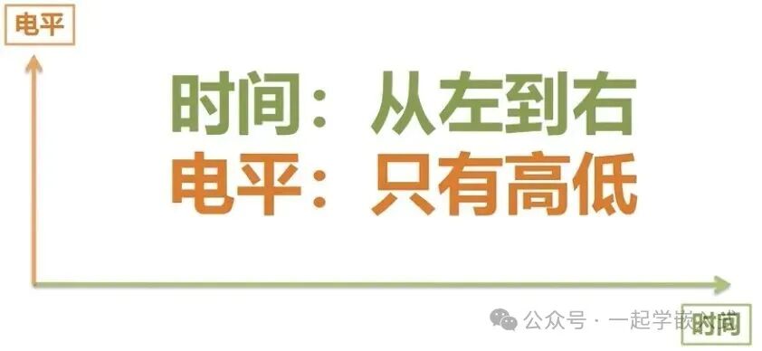
The core of a timing diagram is the relationship between time and the level changes. Time progresses from left to right, and levels are represented as high or low, typically denoted by 0 and 1.
A timing diagram helps us understand the changes of various signals in a circuit and their states at different points in time.
Through timing diagrams, we can clearly display the timing characteristics of digital circuits, such as the start time, duration, trends of changes, and the relationships between changes.
Most Timing Diagram Analysis Techniques
For most timing diagrams, we need to master the following techniques to help us correctly interpret the information in the diagram:
-
From top to bottom: Each waveform line in the diagram usually represents different signal channels or device ports. For example, SCL and SDA in I2C communication, MOSI and MISO in SPI communication, and GPIO control lines. By observing the vertical arrangement, we can clearly see the states of these signals at different points in time.
-
From left to right: Time is the core of the timing diagram, so the diagram represents the progression of time from left to right. When analyzing, we need to focus on how signals change over time; the level changes during different time periods will affect the behavior of the entire system.
Further Analysis Techniques for Timing Diagrams
If the timing diagram has a time scale (such as 0s, 1s, etc.), we can use it to accurately determine the duration of each level. If there is no time scale, we do not need to care about specific time values, just focus on the duration or change patterns of the levels.
For timing diagrams with multiple waveforms, it is advisable to observe the relationships between different signals, identifying master-slave relationships or synchronous and asynchronous signal change patterns.
1. Logical Relationships in Digital Circuits
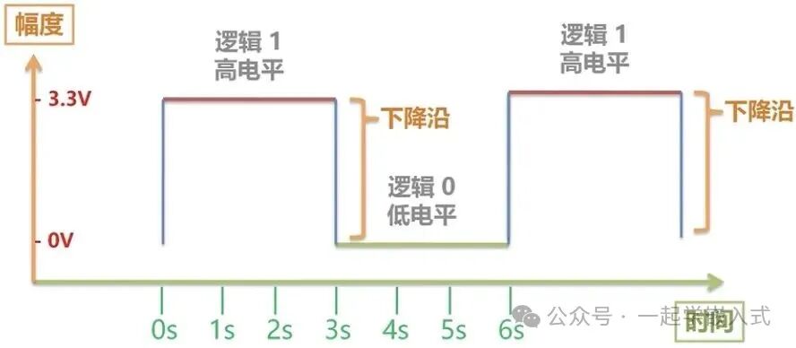
In digital circuits, there are only 0 and 1, representing low and high levels, respectively. The timing diagram expresses the logical state of the circuit at different points in time through the changes in high and low levels.
For example, suppose the timing diagram of a certain signal line is as follows:
- 0-3s: The signal is logic 1 (high level), lasting for 3 seconds.
- 3-6s: The signal is logic 0 (low level), lasting for 3 seconds. This change reflects how the logical state of the signal varies over time.
2. How to Read a Single Waveform Timing Diagram?
When viewing a single waveform, consider the following points:
-
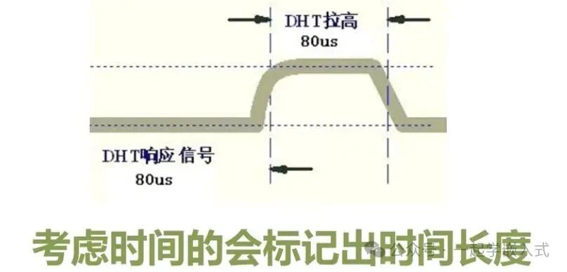
Duration: The timing diagram usually indicates the duration of each level state. If not marked, it means we only care about the high and low levels, and do not need to calculate time precisely.
-
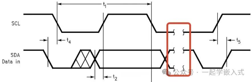
Level Changes: When a level changes from one state to another, there is a certain transition time. For example, the transition from high to low may not happen instantaneously, but will have a transition region (usually represented by slashes or other symbols).Extended Knowledge:
- In actual circuits, level changes typically do not happen instantaneously. We often see that during the transition from high to low or low to high, the waveform will exhibit a slope (i.e., transition time).
- Slashes indicate transition time: The shape and length of these slashes represent the time taken for the level to transition from one state to another. Transition time is especially important in high-speed circuits, as excessive transition time may lead to signal distortion or misjudgment.
-
Physical Changes: Actual level changes are a continuous process, not instantaneous. The slashes and vertical lines in the timing diagram represent the transition or stable state of the level. Unless specifically noted, they have the same meaning, representing a smooth transition of the level from one state to another.
Case 1: Consider that time will indicate the duration; if not marked, we do not need to consider time.
Case 2: The time taken for the level to change from one level to another is represented below, indicating the transition between levels.

Case 3: Physical changes, level changes cannot be instantaneous; they require a certain transition time.

If there are no special markings, then the meanings of the slashes and vertical lines here are the same.
3. Where Do the Levels in Timing Diagrams Come From?
The levels and waveform data in timing diagrams usually come from specific hardware documentation, such as:
Chip data sheets: These will detail the timing characteristics of each pin of the chip, including timing requirements and state changes of input and output signals. For example, how the level of a certain signal line changes with the clock signal.
Protocol specifications: In communication protocols like I2C and SPI, the level changes in timing diagrams are defined by the protocol specifications. Each communication protocol has clear regulations on signal levels, timing, transmission rates, etc.
The level changes in timing diagrams are not only related to the electrical characteristics of the chip itself but also closely related to external devices, environmental factors, and the operating state of the circuit.
4. How to Read Timing Diagrams with Multiple Waveforms?
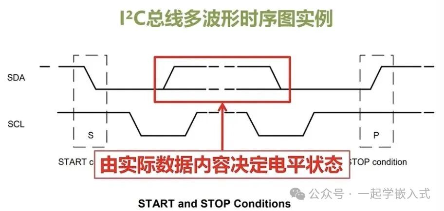
Timing diagrams with multiple waveforms are typically used to represent the level change relationships of multiple signal ports at the same time.
For example, the data transmission process on an I2C bus involves multiple signal lines (such as SCL and SDA) changing levels at different times.
-
Changes in synchronous signals: For protocols like I2C and SPI, timing diagrams can show how different signals change simultaneously. For instance, the changes in the clock (SCL) and data (SDA) lines in I2C are closely related, with the value of SDA being valid only when SCL is low.
-
Dotted sections: Dotted lines in timing diagrams usually represent omitted signals or waveforms, aimed at simplifying the timing diagram and reducing unnecessary complexity. Through dotted lines, we can focus on the main signal changes.
-
Master-slave transmission relationships: Timing diagrams can also help us analyze the signal transmission relationships between the master and slave, such as who initiated the data transmission, when the levels change, and how they synchronize. The relative relationships between waveforms in the timing diagram are crucial, as they can show the order of signal transmission and timing requirements.
Case 1:Multi-waveform diagrams are mainly used to show the level change relationships formed by multiple ports at the same time, such as the I2C bus.
Case 2:The dotted section omits many waveform representations in the middle process, similar to the above representation.
Case 3: The transmission relationship between the master and slave.


5. Timing Diagram Analysis Examples
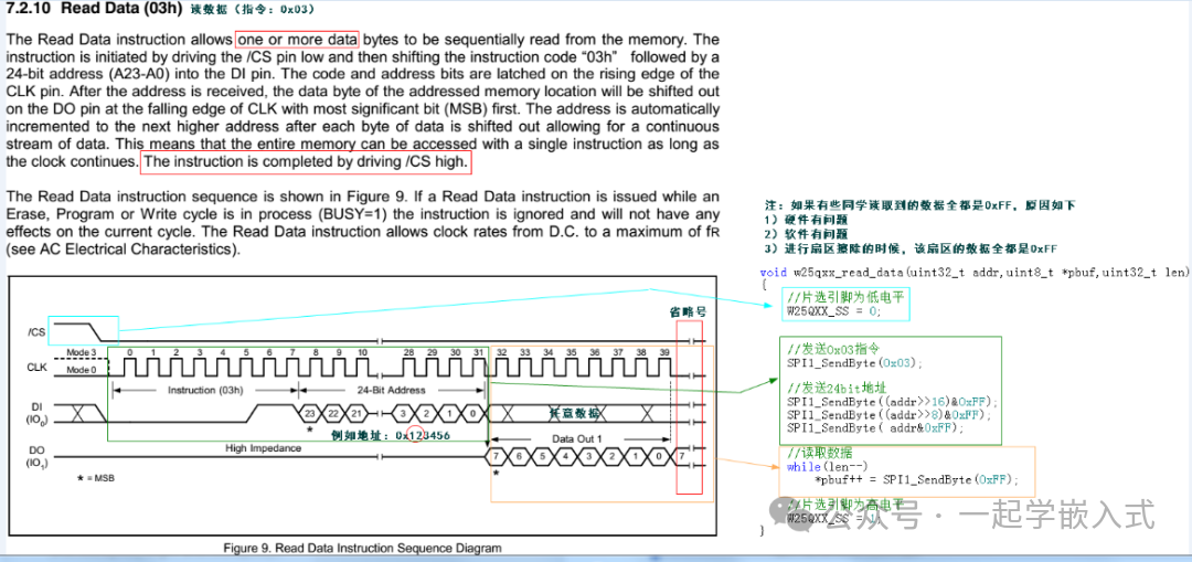
5.1. SPI Timing Diagram
SPI (Serial Peripheral Interface) is a commonly used serial communication protocol, typically with 4 signal lines: MOSI, MISO, SCK, CS.
- MOSI (Master Out Slave In): Data line sent from the master device.
- MISO (Master In Slave Out): Data line sent from the slave device.
- SCK (Clock): Clock signal generated by the master device.
- CS (Chip Select): Used to select the target device.
When analyzing the SPI timing diagram, pay special attention to:
- Clock cycles: The values of MOSI and MISO change within each clock cycle.
- Data transmission order: Data is transmitted bit by bit under the control of the clock signal.
- The timing diagram shows how these signal lines change levels at different points in time.
- The key to the SPI timing diagram is the synchronization of data transmission; the clock signal (SCK) between the master and slave determines the sampling time of the data.
- The waveforms shown in the timing diagram indicate the transmission of data bits within each clock cycle and the states of each signal line.

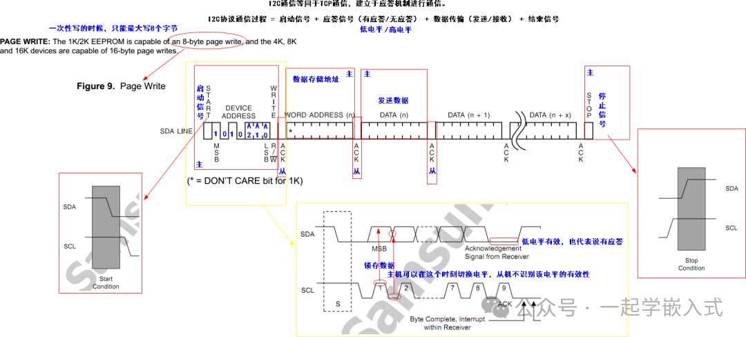
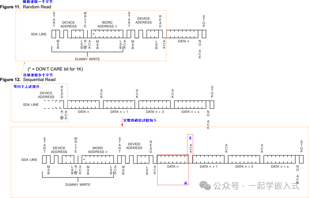
5.2. I2C Timing Diagram
I2C (Inter-Integrated Circuit) is a two-wire serial communication protocol, with signal lines SCL (clock line for synchronous transmission) and SDA (data line for data transmission).
- In the I2C timing diagram, the clock signal (SCL) and data line (SDA) change synchronously.
- The timing diagram will detail how data is written or read during each clock cycle, as well as the markers for START and STOP signals.
These examples of timing diagram analysis can help us better understand the synchronization of signals and data transmission rules in different communication protocols.

Source: Yangtao Electronics & Huqing Yuanjian
This article is sourced from the internet, and the copyright belongs to the original author. If there is any infringement, please contact for removal.

Follow 【Learn Embedded Together】 to become better together!
If you find this article useful, click “Share”, “Like”, “Recommend”!