
32
Single
Chip
Microcontroller
I
O

When it comes to the IO of the 32-bit microcontroller, taking the F1 series as an example, we first need to mention:
1 initialization function:
void GPIO_Init(GPIO_TypeDef* GPIOx, GPIO_InitTypeDef* GPIO_InitStruct);
2 functions to read input levels:
uint8_t GPIO_ReadInputDataBit(GPIO_TypeDef* GPIOx, uint16_t GPIO_Pin);
uint16_t GPIO_ReadInputData(GPIO_TypeDef* GPIOx);
2 functions to read output levels:
uint8_t GPIO_ReadOutputDataBit(GPIO_TypeDef* GPIOx, uint16_t GPIO_Pin);
uint16_t GPIO_ReadOutputData(GPIO_TypeDef* GPIOx);
4 functions to set output levels:
void GPIO_SetBits(GPIO_TypeDef* GPIOx, uint16_t GPIO_Pin);
void GPIO_ResetBits(GPIO_TypeDef* GPIOx, uint16_t GPIO_Pin);
void GPIO_WriteBit(GPIO_TypeDef* GPIOx, uint16_t GPIO_Pin, BitAction BitVal);
void GPIO_Write(GPIO_TypeDef* GPIOx, uint16_t PortVal);


LED Lighting Example

Here, I will mainly teach you how to operate the GPIO of the 32F1 series using a program; taking the LED and button input from the ZhiDian atom as an example, I will explain the two modes of GPIO input and output.
01
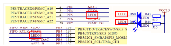
First, observe the schematic diagram, find the IO port connected to the LED, and determine the target to operate. Then proceed to program the IO port.
Enable the IO port clock. Call the function RCC_APB2PeriphClockCmd();
Different IO groups require different clock enable functions.
l Initialize the IO port mode. Call the function GPIO_Init();
l Operate the IO port, output high and low levels.
GPIO_SetBits();
GPIO_ResetBits();

02
Here, we use the knowledge of C language structures to initialize the GPIO_Init() function. To assign values, we first need to enter the definition of GPIO_Init(), select this function, right-click and go to definition to see the interface as shown below.
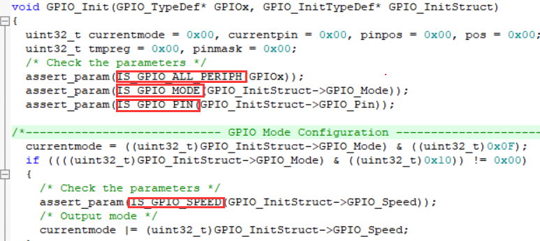
03
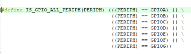
We just need to find the content within the red box, then perform a right-click and go to definition operation to find the parameter options and locations, for example;
04
After copying and assigning the required values, the initialization of the IO port mode is complete, and we can then use bit operations and the functions GPIO_SetBits(); GPIO_ResetBits(); to output high and low levels from the IO port.
The above is about the GPIO output configuration for lighting up an LED.
Button Input Example
Next, let’s look at the input part (button experiment) (taking the Elite as an example).
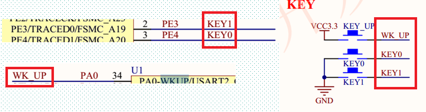
According to the schematic, we can obtain the initialization mode and ideas.
KEY0 KEY1 initialized as pull-up, KEY UP initialized as pull-down.
· Enable the corresponding IO port clock for the button.
Call the function: RCC_APB2PeriphClockCmd();
· Initialize IO mode as pull-up/pull-down input.
Call the function: GPIO_Init();
· Scan the IO port level.
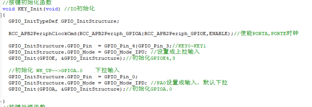
The approach is the same as output, just with different parameter assignments, there is not much difference.
Using the input function, we can obtain the input value of the IO.
uint8_t GPIO_ReadInputDataBit(GPIO_TypeDef* GPIOx, uint16_t GPIO_Pin);
The above is the basic process of input and output operations, as well as the differences between pull-up input, pull-down input, floating input, and analog input.
Differences Among Eight IO Modes of STM32
Recently, while looking at the datasheet, I found that there are as many as 8 types of configurations for GPIO in Cortex-M3: (1) GPIO_Mode_AIN Analog Input (2) GPIO_Mode_IN_FLOATING Floating Input (3) GPIO_Mode_IPD Pull-Down Input (4) GPIO_Mode_IPU Pull-Up Input (5) GPIO_Mode_Out_OD Open-Drain Output (6) GPIO_Mode_Out_PP Push-Pull Output (7) GPIO_Mode_AF_OD Multiplexed Open-Drain Output (8) GPIO_Mode_AF_PP Multiplexed Push-Pull Output.
Summary 1
For beginners, I think these concepts must be clarified. The most commonly encountered are push-pull output, open-drain output, and pull-up input, but I have never summarized these before. Therefore, I will summarize here: Push-pull output: can output high and low levels, connecting to digital devices; the push-pull structure generally refers to two transistors controlled by two complementary signals, where one transistor is always on while the other is off. The high and low levels are determined by the IC’s power supply.
The push-pull circuit consists of two identical transistors or MOSFETs, existing in a push-pull manner in the circuit, each responsible for amplifying the waveform of the positive and negative half cycles. During operation, only one of the two symmetrical power switch tubes is on at a time, resulting in low conduction loss and high efficiency. The output can both sink current to the load and source current from the load. The push-pull output stage improves the circuit’s load capacity and increases switching speed.
For detailed understanding, see the diagram:
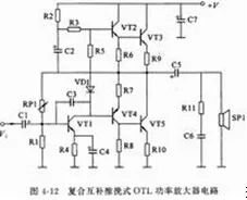
As shown in the figure, the output stage of the push-pull amplifier has two “arms” (two sets of amplifying elements). When the current of one “arm” increases, the current of the other “arm” decreases, and the states of the two alternate. For the load, it seems that one “arm” is pushing while the other is pulling, together completing the current output task. When outputting a high level, that is, when the lower load gate inputs a high level, the output current will be drawn from the power supply through VT3. Thus, when outputting high and low levels, VT3 and VT5 will alternate in operation, reducing power consumption and increasing the capacity of each transistor. Since the conduction resistance of the transistors is very small regardless of which path is taken, the RC time constant is small, and the transition speed is fast. Therefore, the push-pull output stage improves the circuit’s load capacity and increases switching speed.
Open-drain output: The output terminal is equivalent to the collector of a transistor. To achieve a high level state, a pull-up resistor is required. It is suitable for current-type driving.
Its current absorption capability is relatively strong (generally within 20mA).
Open-drain circuits have the following characteristics: 1. Utilize the driving capability of external circuits to reduce the internal driving of the IC. When the internal MOSFET of the IC is turned on, the driving current flows from the external VCC through the pull-up resistor, the MOSFET to GND. The IC only needs a very small gate drive current. 2. Generally, open-drain is used to connect devices of different levels, matching levels, because if the open-drain pin is not connected to an external pull-up resistor, it can only output a low level. If it is necessary to have the function of outputting a high level simultaneously, a pull-up resistor must be connected. A good advantage is that by changing the voltage of the pull-up power supply, the transmission level can be changed. For example, adding a pull-up resistor can provide TTL/CMOS level output, etc. (The resistance value of the pull-up resistor determines the speed of the logic level transition. The larger the resistance, the slower the speed and the lower the power consumption, so the choice of load resistance must consider both power consumption and speed.) 3. OPEN-DRAIN provides a flexible output method, but it also has its weaknesses, which is the delay of the rising edge. Because the rising edge is charged through the external pull-up passive resistor to the load, if the resistor is chosen small, the delay is small, but the power consumption is large; conversely, the delay is large and the power consumption is small. Therefore, if there are timing requirements, it is recommended to use falling edge output. 4. Multiple open-drain output pins can be connected to a single line. Through a single pull-up resistor, a “wired AND” relationship can be formed without adding any devices. This is also the principle of bus occupancy state judgment in I2C, SMBus, etc. Supplement: What is “wired AND”? In a node (line), connect a pull-up resistor to the power supply VCC or VDD and n NPN or NMOS transistors’ collectors C or drains D, with the emitters E or sources S of these transistors connected to ground. As long as one transistor is saturated, this node (line) will be pulled to ground level. Because the base current (NPN) or gate voltage (NMOS) is applied to saturate the transistor, the relationship of these bases or gates to this node (line) is NOR logic. If an inverter is added after this node, it becomes OR logic. It can be simply understood as: when all pins are connected together, an external pull-up resistor is connected, if one pin outputs logic 0, it is equivalent to grounding, and the parallel circuit is “shorted by a wire”, so the external circuit logic level becomes 0, only when all are high levels, the result of AND is logic 1. Regarding push-pull output and open-drain output, I will summarize with the simplest diagram:
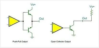
The left side of the diagram is the push-pull output mode, where when the comparator outputs a high level, the lower PNP transistor is off while the upper NPN transistor is on, outputting a high level VS+; when the comparator outputs a low level, the situation is reversed, the PNP transistor is on, and the output is connected to ground, resulting in a low level. The right side can be understood as the open-drain output form, which requires a pull-up.
Floating input: For floating input, I have not found a very authoritative explanation, so I can only understand it from the following diagram.
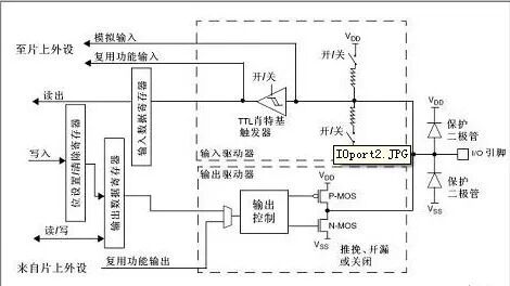
Since floating input is generally used for external button inputs, combined with the input circuit shown in the diagram, I understand that in the floating input state, the IO level state is uncertain and is entirely determined by external input. If the pin is floating, reading the level of that port is uncertain. Pull-up input/pull-down input/analog input: These concepts are easy to understand and can be easily read from the literal meaning. Multiplexed open-drain output, multiplexed push-pull output: can be understood as the configuration situation when the GPIO port is used for a second function (i.e., not used as a general IO port).
Summary 2
In STM32, select IO modes (1) Floating Input_IN_FLOATING – floating input, can be used for KEY recognition, RX1 (2) Pull-Up Input_IPU – IO internal pull-up resistor input (3) Pull-Down Input_IPD – IO internal pull-down resistor input (4) Analog Input_AIN – used for ADC analog input, or low power mode for energy saving (5) Open-Drain Output_OUT_OD – IO outputs 0 to GND, IO outputs 1, floating, requiring an external pull-up resistor to achieve high level output. When outputting 1, the state of the IO port is pulled high by the pull-up resistor, but since it is in open-drain output mode, this IO port can also be changed to low level or remain unchanged by external circuits. It can read the IO input level changes, achieving the bidirectional function of IO in C51 (6) Push-Pull Output_OUT_PP – IO outputs 0 to GND, IO outputs 1 to VCC, reading input values is unknown (7) Multiplexed Push-Pull Output_AF_PP – internal peripheral function (I2C SCL, SDA) (8) Multiplexed Open-Drain Output_AF_OD – internal peripheral function (TX1, MOSI, MISO, SCK, SS) STM32 setting examples: (1) Use open-drain output_OUT_OD for analog I2C, connect a pull-up resistor, can correctly output 0 and 1; when reading values, first GPIO_SetBits(GPIOB, GPIO_Pin_0); pull high, then read the IO value; use GPIO_ReadInputDataBit(GPIOB, GPIO_Pin_0); (2) If there is no pull-up resistor, the IO defaults to high level; to read the IO value, you can use pull-up input_IPU and floating input_IN_FLOATING and open-drain output_OUT_OD; usually, there are 5 ways to use a certain pin function, and their configuration methods are as follows: 1) As a general GPIO input: configure the pin as floating input, weak pull-up input, or weak pull-down input as needed, while not enabling all corresponding multiplexing function modules for that pin. 2) As a general GPIO output: configure the pin as push-pull output or open-drain output as needed, while not enabling all corresponding multiplexing function modules for that pin. 3) As a general analog input: configure the pin as analog input mode, while not enabling all corresponding multiplexing function modules for that pin. 4) As an input for built-in peripherals: configure the pin as floating input, weak pull-up input, or weak pull-down input as needed, while enabling a certain multiplexing function module corresponding to that pin. 5) As an output for built-in peripherals: configure the pin as multiplexed push-pull output or multiplexed open-drain output as needed, while enabling all corresponding multiplexing function modules for that pin. Note that if there are multiple multiplexing function modules corresponding to the same pin, only one can be enabled, and the others must remain disabled. After reset, the IO ports of STM32 are in input floating state. After resetting the JTAG pins, they are in pull-up or pull-down state. All IO ports have external interrupt capability, and the ports must be configured in input mode to use the external interrupt function.
IO Port Multiplexing Function Configuration:
For multiplexing function inputs, the port can be configured as any input mode or multiplexing function output mode. For multiplexing function outputs, the port must be configured as multiplexing function output. For bidirectional multiplexing functions, the port must be configured as multiplexing function output. Some IO ports of STM32 can be remapped to other multiplexing functions. STM32 has a GPIO locking mechanism, which locks the GPIO configuration and cannot be modified before the next reset. When the LSE oscillator is off, OSC32_IN and OSC32_OUT can be used as general IO PC14 and PC15. When entering standby mode or the backup domain is powered by Vbat, the functions of PC14 and PC15 are lost, and these two IO port lines are set to analog input function. OSC_IN and OSC_OUT can be remapped to GPIO PD0, PD1. Note that PD0 and PD1 can only be used for 50MHz output mode when outputting ground. Note: PC13, PC14, PC15 can only be used for 2MHz output mode, and can carry a maximum load of 30pF, and only one pin can be used at the same time!!!!!!!!

Some Screenshots from Electronic Books

【Complete Set of Hardware Learning Materials Collection】