Cover | Electronic Transformer and Inductor Network
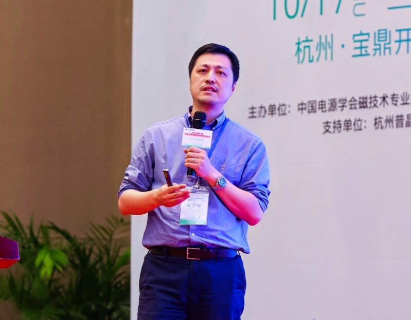
At the 11th Joint Academic Annual Conference on Power Converter Magnetic Components in 2024, Professor Wang Ningning, Vice Chairman of the Magnetic Technology Professional Committee of the China Power Supply Society and Hangzhou University of Electronic Science and Technology, delivered an impressive speech titled “New Packaging Substrate Integration Technology”.
 Professor Wang Ningning
With the rapid development of digital processing chips such as CPUs, GPUs, and FPGAs, power systems are undergoing unprecedented transformation. Against this backdrop, Professor Wang Ningning’s speech and the subsequent interview not only have theoretical value but also provide guidance for industrial practice.
After the conference, Professor Wang was interviewed by reporters from the Electronic Transformer and Inductor Network, discussing topics such as the future development of inductors, technology applications, and industrialization challenges.
Transformation of Power Systems: Why is Magnetic Integration Technology Key?
With the trend of vertical power supply development, traditional power systems are gradually transforming towards miniaturization, thinness, high frequency, and integration to meet the growing power supply demands of digital processing chips such as CPUs, GPUs, and FPGAs.
The multi-core trend of these digital processing chips not only enhances computing power but also raises more refined requirements for power management, aiming to improve energy management efficiency, extend battery life, or reduce power consumption.
Currently, power supply systems still primarily rely on board-level power supply, where the power conduction path is crucial for power efficiency and performance, especially in terms of current change rate (DI/DT) and output voltage stability. Therefore, reducing the loss and self-impedance of the power distribution network (PDN) path has become a key issue to be solved in the power field.
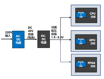
Technological evolution has prompted profound changes in power architecture, shifting from traditional 12V to low-voltage power supply modes of 1-5V, gradually transitioning to 48V to 1.55-3.3V low-voltage bus architecture. This architecture enables low-voltage buses to power digital chips, facilitating the realization of on-chip power supplies (IVR) or fully integrated power supplies (FIVR).
Professor Wang Ningning
With the rapid development of digital processing chips such as CPUs, GPUs, and FPGAs, power systems are undergoing unprecedented transformation. Against this backdrop, Professor Wang Ningning’s speech and the subsequent interview not only have theoretical value but also provide guidance for industrial practice.
After the conference, Professor Wang was interviewed by reporters from the Electronic Transformer and Inductor Network, discussing topics such as the future development of inductors, technology applications, and industrialization challenges.
Transformation of Power Systems: Why is Magnetic Integration Technology Key?
With the trend of vertical power supply development, traditional power systems are gradually transforming towards miniaturization, thinness, high frequency, and integration to meet the growing power supply demands of digital processing chips such as CPUs, GPUs, and FPGAs.
The multi-core trend of these digital processing chips not only enhances computing power but also raises more refined requirements for power management, aiming to improve energy management efficiency, extend battery life, or reduce power consumption.
Currently, power supply systems still primarily rely on board-level power supply, where the power conduction path is crucial for power efficiency and performance, especially in terms of current change rate (DI/DT) and output voltage stability. Therefore, reducing the loss and self-impedance of the power distribution network (PDN) path has become a key issue to be solved in the power field.
Technological evolution has prompted profound changes in power architecture, shifting from traditional 12V to low-voltage power supply modes of 1-5V, gradually transitioning to 48V to 1.55-3.3V low-voltage bus architecture. This architecture enables low-voltage buses to power digital chips, facilitating the realization of on-chip power supplies (IVR) or fully integrated power supplies (FIVR).
Fully Integrated Power Supplies Have Significant Advantages.
First, by utilizing micro-nano processing or packaging technology, passive components such as inductors and capacitors are integrated into a single chip, greatly reducing the power supply area and height, allowing them to be placed inside the load package or its backplane, thus significantly shortening the PDN path;
Second, the enhancement of power granularity allows a single power supply to be decomposed into dozens or even hundreds of independently controlled small power supplies, each capable of independent voltage control, achieving more precise voltage management;
Moreover, the enhancement of dynamic response and reduction of PDN conduction loss significantly improve system efficiency.
However, high frequency, high efficiency, and the integration and miniaturization of magnetic components remain major challenges facing current power design. How to achieve miniaturization and integration of magnetic components while maintaining high performance has become a focus of industry attention.
New Advances in Magnetic Components: Packaging Substrate Magnetic Integration Technology
In traditional board-level power design, independent components such as inductors, capacitors, and controllers are commonly found.
However, with continuous technological advancements, about a decade ago, revolutionary changes emerged in the market—inductors were cleverly embedded within the chip packaging, significantly reducing the circuit board area.
This trend has not stopped; in recent years, we have witnessed the simultaneous integration of inductors and capacitors into the packaging, representing a technological breakthrough that further promotes the reduction of power supply area.
Ultimately, an ideal vision is gradually being realized: integrating power control circuits, power devices, magnetic components, and capacitors all on the same silicon chip, forming what is known as “on-chip integrated power supply.”
Although this technology holds great promise, its development process still faces numerous challenges, requiring more innovations and breakthroughs.
In the field of magnetic component magnetic integration technology, we have also witnessed the evolution from winding-type magnetic components, flat magnetic components, to PCB-integrated magnetic components, and even silicon-integrated magnetic components. This series of developments not only improves the performance of magnetic components but also provides a solid foundation for the integration of power systems.
Meanwhile, the embedded packaging substrate in packaging integration technology, along with the combined magnetic integration technology, demonstrates exceptional application potential.
Packaging Integrated Power Supplies greatly reduce the space occupied by power systems by integrating passive components such as inductors and capacitors with control chips within the same package.
Meanwhile, on-chip integrated power supplies, as the ultimate goal of power technology, require the integration of all passive components and control chips into a single chip at higher frequencies, which undoubtedly poses a significant challenge to current technology.
In the practical exploration of packaging integrated power supplies, various integration methods and forms have emerged, each with its own characteristics in frequency response, process complexity, supply chain maturity, and development cycle.
For example, silicon-based integrated power supplies are known for their high precision and flexibility, but the corresponding equipment requirements and process complexity are also high; while PCB-integrated power supplies are favored for their simple processes, mature supply chains, and short development cycles, yet they have certain limitations in terms of integration and precision.
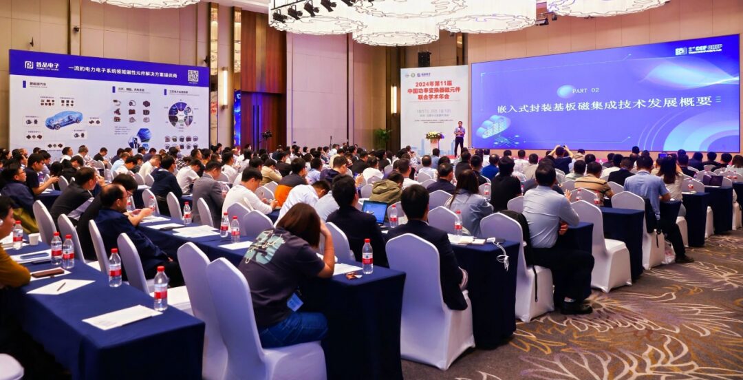
Professor Wang Ningning delivering a speech at the academic annual conference
In industry practice, technology giants such as Intel are also actively exploring different technological paths. One solution is to use air-core inductors, which achieve efficient and high-frequency applications of fully integrated power supplies with their small inductance and operating frequencies of up to 100MHz to 140MHz.
Another solution combines magnetic core structures with PCB technology, by drilling holes in the PCB substrate and filling them with magnetic powder cores to form single-turn inductor structures, effectively realizing vertical power supply.
Although this structure has relatively low inductance and is subject to process and material limitations, with the magnetic core permeability only at 8.5, it is still suitable for higher frequency switching power supplies, such as 90MHz to 100MHz.
However, this technology also faces some challenges. The thickness of the PCB is relatively thick, and the filler is prone to cracking during the lamination process, affecting the reliability of the product.
Moreover, due to process limitations, the height of the inductance produced is difficult to reduce, especially when the design relies on height to achieve sufficient inductance. Therefore, in existing solutions, the size of the PCB generally exceeds 1.0mm.
Professor Wang Ningning’s Team: Exploring the Challenges and Innovations of Packaging Substrate Magnetic Integration
In response to the above issues, Professor Wang Ningning and his team have conducted extensive exploratory work. They attempted to make intermediate vias in the PCB, where the upper and lower wires are still made through the PCB, but the middle is excavated to insert different magnetic materials, such as thin film materials or powder core materials.
The researchers created two types of magnetic cores: iron-silicon-aluminum powder cores and nickel-iron thin films.
The iron-silicon-aluminum powder core is wrapped with an insulating layer through surface treatment and then hot-pressed into blocks, which are then cut into thin slices to be placed in the PCB holes; the nickel-iron thin film is produced on a PI substrate through electroplating, and after multi-layer lamination and cutting, it is filled into the holes.
These two types of inductors exhibit different characteristics:
The iron-silicon-aluminum powder core has good high-frequency characteristics, with a Q value of up to 36, suitable for frequency ranges of 50MHz to 100MHz; while the nickel-iron thin film has higher inductance, but higher eddy currents at high frequencies, resulting in a relatively low Q value of about 16.
To reduce PCB thickness, they adopted a thinner process, using 6-micron nickel-iron alloy materials, which are bonded and hot-pressed into multi-layer films, then cut into small pieces to be placed in PCB holes.
The inductors made using this method exhibit characteristics similar to previous thin-film inductors, with inductance values between 20 and 30 nH, and Q values in the teens, with a thickness significantly thinner than the previous drilling method, with an overall thickness of less than 0.4mm.
The research team also attempted to make magnetic films into sheets and integrate them with PCB processes. They first stacked and pressed the magnetic films, then patterned them, and filled the holes with adhesive. This method can further reduce the reserved safety distance and form thinner flexible board integrated inductors through normal PCB processes.
They used PI films and electroplated on both sides, controlling the thickness to around 2 microns to further enhance high-frequency performance.
Results showed that at tens of megahertz, the inductance decreased and the Q value significantly increased, reaching around 20, with the frequency at which the Q value occurred increasing to 15 megahertz.
The research team compared flexible boards or ultra-thin PCBs with previous work, finding that within the operational range of 10MHz to 20MHz, the Q value remains competitive.
However, due to the lack of high-precision packaging substrate processes, the inductance density is relatively low. If more precise packaging substrate processes are adopted, the area can be significantly reduced, and the inductance density can be increased.
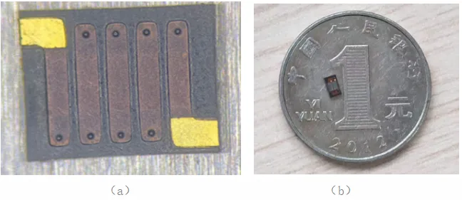 Magnetic integrated devices: (a) Packaging substrate integrated inductors (b) Silicon-based integrated inductors
In addition, the research team also explored the use of drilled holes for impedance testing under high-frequency signals and attempted to extract losses from magnetic cores.
They found that traditional round sample testing methods are not suitable for thin film materials with varying shapes, thus the PCB-based method provides a new idea for testing thin film magnetic core losses.
Currently, Professor Wang Ningning and his research team can accurately test the losses of thin film magnetic cores in the range of 10MHz to 60MHz.
Wang Ningning believes that in terms of future development and challenges, research on high-frequency ultra-low loss thin film/powder cores and large-scale preparation, high-frequency loss testing of thin film soft magnetic materials, efficient magnetic component integration process technologies, precise mathematical models for high-frequency inductors, and overall packaging technology for power systems are urgent issues that need to be addressed.
Interview Highlights: Future Outlook for Packaging Substrate Magnetic Integration Industrialization
In his speech, Professor Wang profoundly analyzed the challenges faced by the transformation of power systems and fully integrated power supplies in an easy-to-understand manner, introduced the latest progress in embedded packaging substrate magnetic integration technology, and forecasted the future development trends of silicon-based magnetic integration devices, providing many profound insights and inspirations to the attending magnetic component enterprises.
Everyone showed great enthusiasm and curiosity about the future application scenarios of this technology and the challenges that may be encountered on the path to industrialization. Based on this, the reporters from the Electronic Transformer and Inductor Network specially invited Professor Wang for an interview, where he provided detailed answers to the concerns of industry enterprises.
Reporter: What aspects of technical research are currently being conducted regarding the future development of inductors?
Wang Ningning:We are currently researching two types of technologies: packaging integrated inductors and silicon-based inductors. Packaging integrated inductors integrate inductors and other passive components with connection lines and structural components to form a complete packaging integration solution.
Silicon-based inductors, on the other hand, directly grow wires and magnetic core material insulation layers on top of control chips through thin film growth and other micro-nano processes, achieving on-chip power integration.
Reporter: How do you view the perspective of air inductors as a future development trend?
Wang Ningning:I believe that air inductors do have certain advantages in some scenarios, such as being relatively easy to implement and having a relatively complete industrial chain. However, as a power designer or application party, we will still choose the most suitable inductor solution based on specific needs.
Air inductors may have some performance losses, so we need to weigh the pros and cons to make decisions. Meanwhile, with continuous technological advancements and the maturation of the industrial chain, more and better inductor solutions may emerge in the future.
Reporter: What applications do you see for the technical solutions you shared in the future?
Wang Ningning:We have not yet truly invested in product manufacturing; we are only conducting technical discussions in this area. Based on our current research, this technology is feasible. If we really want to implement this solution for mass production in the future, the entire industrial chain for this packaging substrate solution will be relatively complete.
Moreover, from the entire development process, if the supply chain is complete in the future, the product development cycle will be relatively short.
Although we do not yet have specific products, I can say that this technology can power AI chips, or CPUs, GPUs, and other digital processing chips requiring high power density, high efficiency, and power space limitations. Such products can all utilize our technology.
Reporter: What do you think are the main technical challenges faced by companies in the process of industrialization?
Wang Ningning:I think the main challenges lie in the maturity of the technology and the integration capability of the industrial chain. Although some technologies seem promising, they have not yet formed a mature industrial chain and solution.
This requires companies to have strong R&D capabilities and resource integration abilities to promote the industrialization and application of technologies. At the same time, domestic companies generally hold a cautious attitude towards new technologies and are reluctant to be the first to take risks.
Reporter: I heard that your research team has already cooperated with enterprises; can you reveal which companies they are?
Wang Ningning:Of course. We have cooperation with companies such as OPPO and China Electronics Corporation. These collaborations enable us to better transform research results into practical applications and provide strong support for the innovative development of enterprises; I would like to express my heartfelt thanks for the strong support from these companies.
Reporter: Can you share the next research direction or core objectives?
Wang Ningning:Our current research direction is two-pronged: on one hand, we continue to advance the research and application of packaging integrated inductors to provide technical support for the integration of inductors in vertical power supply and module power; on the other hand, we are also actively exploring silicon-based inductors to provide solutions for ultimately achieving on-chip integrated power supplies.
Professor Wang Ningning and his research team have achieved significant research results in packaging integrated inductors and silicon-based inductors. These results not only provide strong support for innovation in power technology but also offer feasible solutions for future high-performance chip power supply needs.
Companies need to focus on technological innovation, ensuring high performance while achieving miniaturization and integration of magnetic components. At the same time, they need to balance supply chain maturity, process complexity, and development cycles, strengthen industry-university-research cooperation, and transform research results into practical applications to meet the higher demands of AI and high-performance computing fields for power systems.
In the future, power technology will continue to innovate, and the industrialization and application of magnetic component technology will inject new momentum into technological development.
Confronted with the trends of miniaturization, high frequency, and integration in power systems, what do you think is the biggest challenge facing current magnetic integration technology?
Does the new packaging substrate integration technology proposed by Professor Wang Ningning provide new ideas or solutions for your R&D work? Welcome to share your views and experiences!
This article is an original article from the Electronic Transformer and Inductor Network, and may not be reproduced without authorization; otherwise, legal responsibility will be strictly pursued.
Click to follow for more information on electronic transformers and inductors
— Previous Recommendations —
Disclaimer: The content is sourced from the internet, WeChat public accounts, and other public channels. We maintain a neutral stance on the viewpoints expressed in the text. This article is for reference and communication only. The copyright of reproduced manuscripts belongs to the original authors and institutions. If there is any infringement, please contact us for deletion.
Company Profile:Shenzhen Saimein Technology Co., Ltd. (referred to as Saimein Technology) is located in the XinQiao Comprehensive Building, Bao’an District, Shenzhen. The company’s R&D team has successfully developed graphene metallization technology and large-scale preparation technology for graphene. The companybuilt a soft board graphene metallization production line in Shenzhen in April 2018,and in October 2019, its subsidiary Dongguan Saimein Technology Co., Ltd. built a production line with an annual output of 50 tons of graphene slurry, which has been successfully put into production, gradually promoting the application of graphene metallization technology in circuit boards, electronic shielding, plastic electroplating metallization,ppfilm metallization, composite materials, and other fields of research and industrialization promotion, striving to become a technological new star in the new energy and new materials industry within 3-5 years, using new technologies and materials to change relevant electronics and surface treatment industries, promote environmentally friendly new technologies, reduce environmental pollution, and continuously promote the progress and development of related industries’ technological advancements.
Business Consultation Phone:
Mr. Chen:13823133110
Mr. Yang:13714337073
Company Landline:0755-23593156
Company Address:Room 908, XinQiao Comprehensive Building, Beihuan Road, XinQiao Street, Bao’an District, Shenzhen