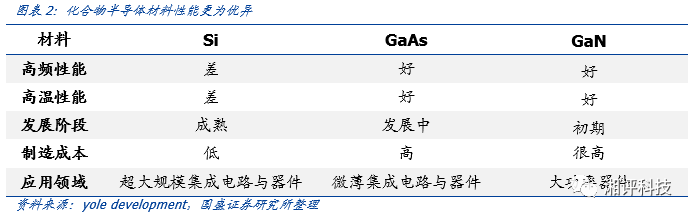
Semi-conductor materials can be divided into two categories: elemental semiconductors and compound semiconductors. The former includes semiconductors formed from elements such as silicon (Si) and germanium (Ge), while the latter includes compounds such as gallium arsenide (GaAs), gallium nitride (GaN), and silicon carbide (SiC). In the past, semiconductors have undergone three generations of changes, gallium arsenide (GaAs), gallium nitride (GaN), and silicon carbide (SiC) semiconductors represent the second and third generations, respectively. Compared to first-generation semiconductors, they have much better high-frequency and high-temperature performance, although they are more expensive to manufacture, making them the new elite in the semiconductor industry.
Among the three major compound semiconductor materials, GaAs holds the largest market share, mainly used in the communications field, with a global market capacity close to $10 billion, primarily benefiting from upgrades in communication RF chips, especially PAs; GaN has superior power and high-frequency performance and is mainly used in military applications, with a current market capacity of less than $1 billion, but is expected to see widespread applications as costs decrease; SiC is mainly used as a high-power semiconductor material in automotive and industrial power electronics, offering significant advantages in high-power conversion applications.
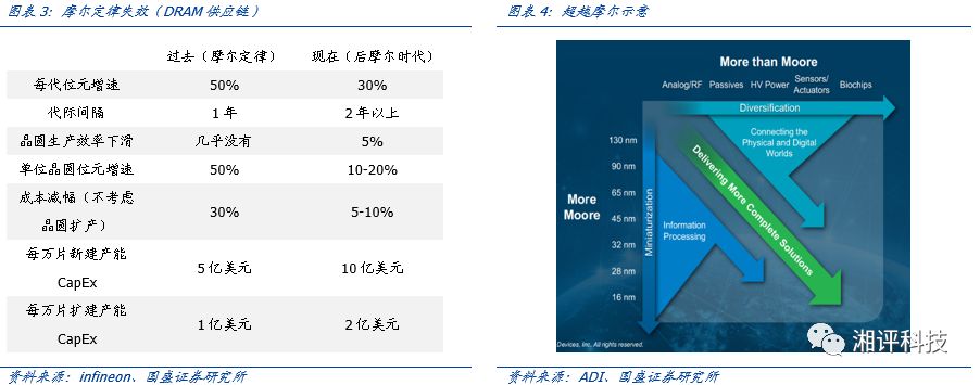
Moore’s Law is slowing down, leading to a differentiation in the development of integrated circuits. Currently, the development of integrated circuits mainly has two directions: More Moore (deep Moore) and More than Moore (beyond Moore). Moore’s Law states that approximately every 18 months, the number of transistors on a chip doubles while the price halves. However, at 28nm, it encountered obstacles; although the number of transistors doubled, the price did not drop by half. More Moore (deep Moore) refers to the continued improvement of process node technology, entering the post-Moore era. Meanwhile, More than Moore (beyond Moore) has been proposed, which focuses on achieving more applications by adding more functionalities to a single IC.
Analog ICs are more suitable for the More than Moore (beyond Moore) path. Advanced processes and high integration can enhance the performance and reduce costs of digital ICs, but this does not apply to analog ICs. Analog circuits, such as RF circuits, often require large inductors, and the integration level of advanced processes has little effect while increasing costs; advanced processes are often used in low-power environments, but RF and power analog ICs operate in high-frequency and high-power domains, where advanced processes can even have a negative impact on performance; the linearity of analog circuits under low power and voltage is also difficult to guarantee. The main technology for PAs is GaAs, while the main technology for switches is SOI. More than Moore (beyond Moore) can achieve a combination of different technologies and processes, providing a pathway for further development of analog ICs.
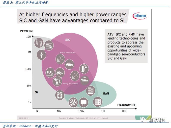
Third-generation semiconductors adapt to more application scenarios. Silicon-based semiconductors have characteristics such as high-temperature resistance, good radiation resistance, ease of fabrication, and high reliability, making over 99% of integrated circuits made from silicon. However, silicon-based semiconductors are not suitable for high-frequency and high-power applications. In the 2G, 3G, and 4G eras, the main material for PAs was GaAs, but in the 5G era, the main material is GaN. The higher frequency of 5G and its leapfrog reflection characteristics result in shorter transmission distances. Due to the high power requirements of millimeter waves, GaN, with its small size and high power characteristics, is currently the most suitable PA material for the 5G era. Third-generation semiconductors like SiC and GaN will better meet future application demands.
Analog ICs focus on voltage and current control, distortion rate, power consumption, reliability, and stability, requiring designers to consider the impact of various components on the performance of analog circuits, making design more challenging. Digital circuits pursue computational speed and cost, often using CMOS technology, and have been following Moore’s Law for many years, continuously adopting more efficient algorithms to process digital signals or using new technologies to increase integration and reduce costs. However, overly advanced process nodes are often detrimental to achieving low distortion and high signal-to-noise ratios or meeting the requirements of outputting high voltage or large current to drive other components, so the evolution of nodes is relatively less demanding for analog ICs compared to digital ICs. The lifecycle of analog chips is also longer, often lasting over 10 years, as evidenced by Fairchild’s operational amplifier μA741, which has been sold for nearly fifty years with ongoing customers.
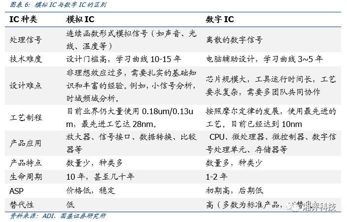
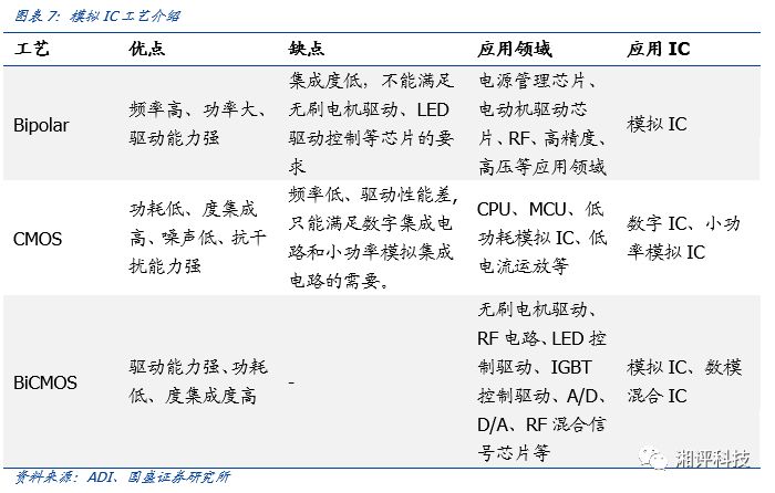
Currently, digital ICs mainly use CMOS technology, while analog ICs employ a variety of processes, free from the constraints of Moore’s Law. The manufacturing processes for analog ICs include Bipolar, CMOS, and BiCMOS technologies. In high-frequency domains, SiGe, GaAs, and SOI technologies can also be combined with Bipolar and BiCMOS processes to achieve superior performance. In power domains, SOI and BCD (BiCMOS-based integration of DMOS and other power devices) processes also perform better. Analog ICs are widely used, and their application scenarios vary, leading to corresponding changes in manufacturing processes.
Compared to first-generation silicon semiconductors, gallium arsenide has high-frequency, radiation resistance, and high-temperature resistance characteristics, making it widely used in mainstream commercial wireless communication, optical communication, and military applications. The popularity of wireless communication and the limitations of silicon’s high-frequency characteristics have contributed to the prominence of gallium arsenide, leading to its large-scale application in the wireless communication field.
Baseband and RF modules are core components that complete 3/4/5G cellular communication functions. RF modules generally consist of transceivers and front-end modules (PA, Switch, Filter). Among them, gallium arsenide has become the mainstream material for PAs and switches.
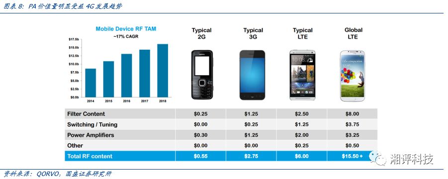
The continuous increase in 4G/5G frequency bands drives the growth in PA usage. Since a single PA chip can only handle signals within a fixed frequency band, an increase in cellular communication frequency bands significantly boosts the consumption of PAs in smartphones. With the popularity of 4G communication, the number of frequency bands expanded from 6 in 2010 to 43, and in the 5G era, it is expected to exceed 60. Currently, mainstream 4G communication uses 5 frequency bands and 13 modes, averaging 7 PAs and 4 RF switches per device.
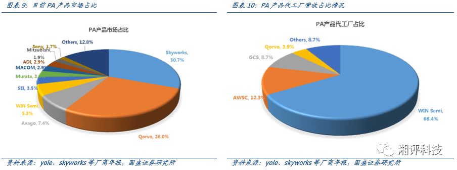
Currently, leading gallium arsenide companies mainly operate under the IDM model, including American companies Skyworks, Qorvo, Broadcom/Avago, Cree, and Germany’s Infineon. At the same time, we also notice that the industry’s development model is gradually shifting from IDM to design + foundry production, with a typical trend being the continuous increase in foundry ratios and Avago selling its Colorado plant to Winsemi last year. We believe that the continuous maturation and standardization of GaAs substrate and device technology, along with significant diversification of products and the value of device design, are leading to an increase in the division of labor between design and manufacturing.
According to estimates from third-party research institutions like Yole Development, the global market size for GaAs devices used in PAs reached $8-9 billion in 2017, with most market share concentrated among three giants: Skyworks, Qorvo, and Avago. It is expected that with communication upgrades, the market will officially exceed $10 billion in the next two years.
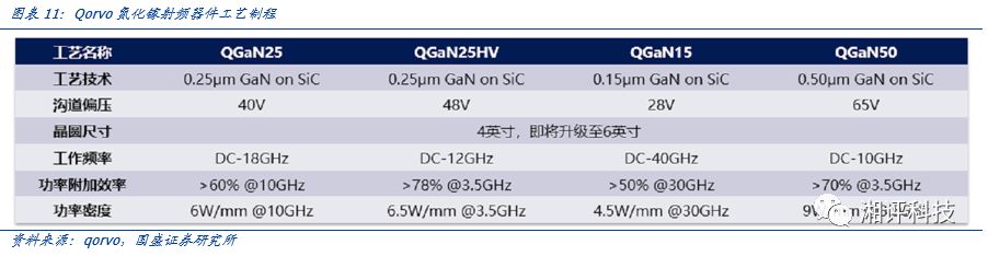
At the same time, the application market does not require advanced process technology below 60 nm line width, and not pursuing the most advanced process technology is another characteristic. Compound semiconductors are aimed at RF, high-voltage, high-power, and optoelectronic fields, without the need for advanced processes. GaAs and GaN devices mainly use processes above 0.13 and 0.18μm. Qorvo is currently developing a 90nm process. Additionally, due to the size limitations of GaAs and SiC substrates, current production lines are primarily 4-inch and 6-inch. Taking Qorvo as an example, we found that the line width of gallium nitride processes is generally between 0.25-0.50um, with production lines mainly being 4 inches.
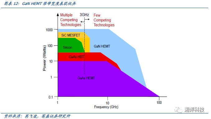
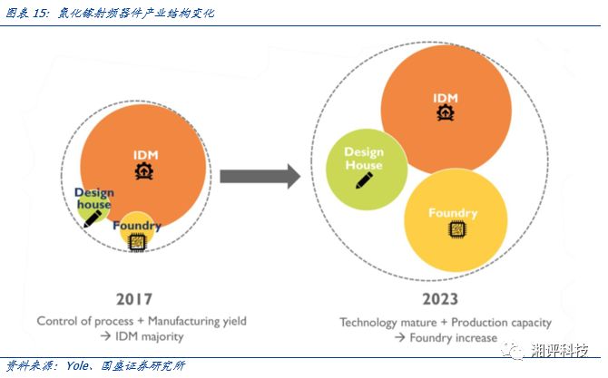
Gallium nitride (GaN) and silicon carbide (SiC) are known as the twin pillars of third-generation semiconductor materials. Due to their differing performance characteristics, their application fields also vary. Gallium nitride, with its wide bandgap, high breakdown field, high saturation electron velocity, high thermal conductivity, stable chemical properties, and strong radiation resistance, has become one of the preferred materials for high-temperature, high-frequency, and high-power microwave devices.
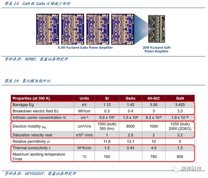
Currently, two-thirds of gallium nitride devices are used in military electronics, such as military communications, electronic interference, and radar; in civilian fields, gallium nitride is mainly applied in communication base stations and power devices. Gallium nitride-based PA amplifiers are more efficient than those made from other materials, saving a significant amount of electricity, and they can almost cover all frequency bands in wireless communication, with high power density, reducing the size and weight of base stations.
The rise of specialty process foundries is a trend driven by division of labor. The global semiconductor industry is divided into two business models: IDM (Integrated Device Manufacture) and vertical division of labor. Due to historical reasons, many established companies mainly operate under the IDM model. With advancements in integrated circuit technology and the limits of Moore’s Law approaching, the technical and financial barriers for each segment are increasing, revealing the disadvantages of the traditional IDM model. New companies often choose the Fabless model to pursue growth more lightly. Simultaneously, older companies like Infineon, TI, and AMD are gradually outsourcing all or part of their manufacturing and testing processes, transitioning to Fab-Lite or even Fabless models.
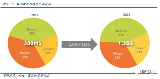
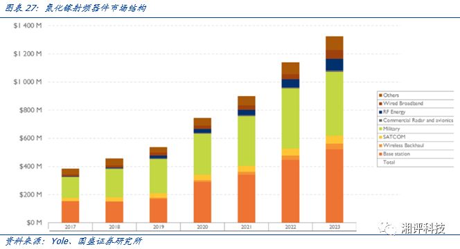
The gallium nitride RF device market is growing rapidly, with a compound annual growth rate of 23%, and the overall structure of the downstream market remains stable. Research firm Yole Development indicates that the gallium nitride RF market size was $380 million in 2017 and is expected to grow to $1.3 billion by 2023, with a compound annual growth rate of 22.9%. The downstream application structure remains stable, mainly focusing on communications and military applications, which together account for about 80%.
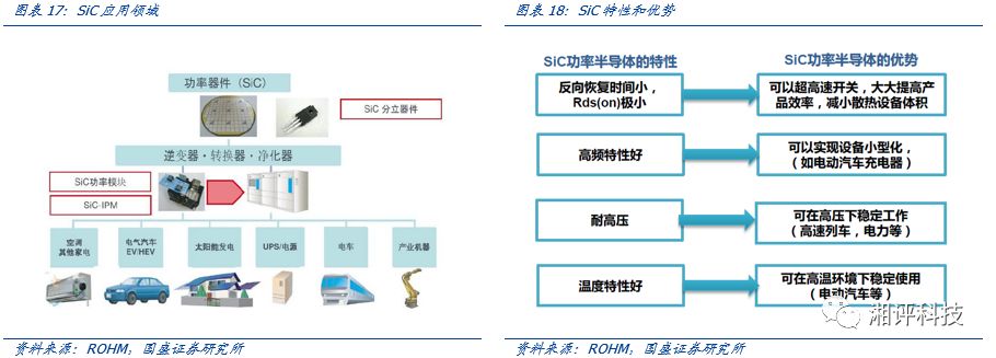
SiC is mainly used in high-power, high-frequency power devices. Diodes, MOSFETs, IGBTs, and other devices made from SiC are expected to replace silicon in automotive electronics in the future. Currently, SiC semiconductors are still in the early stages of development, with material dislocations occurring during wafer growth, leading to decreased reliability of SiC devices. On the other hand, the difficulty in wafer growth results in high prices for SiC materials, and it is expected that significant technological improvements will be needed before widespread application can occur.
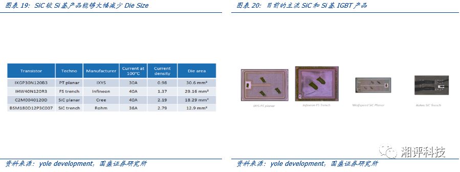
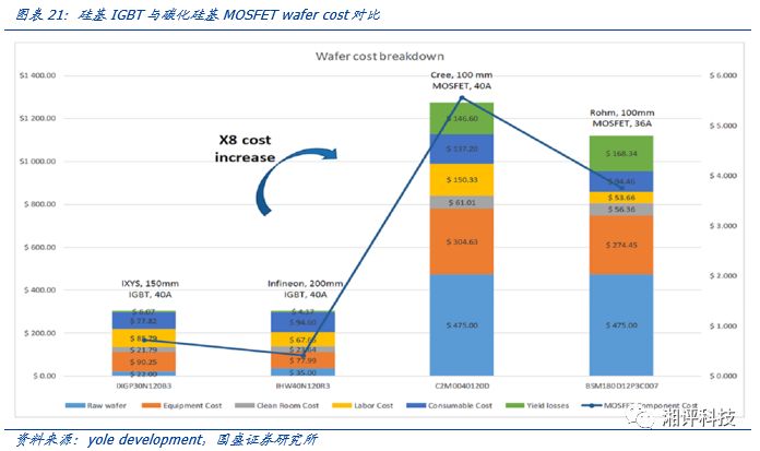
Die Size and cost are the core variables for the industrialization of silicon carbide technology. We compared the current mainstream 1200V silicon-based IGBTs with SiC-based MOSFETs and found that SiC-based MOSFETs significantly reduce Die Size while performing better than silicon-based products. However, the biggest obstacle remains wafer cost, with Yole Development estimating that the cost per wafer for SiC is 7-8 times higher than that of silicon-based products.
Research firm IHS predicts that by 2025, the market size for SiC power semiconductors is expected to reach $3 billion. In the next ten years, SiC devices will begin to be widely used in industrial and electric vehicle fields. Looking at the global SiC market, power electronics accounted for the largest market share from 2016-2017. The main driving factor for this market growth is the increasing use of SiC devices in power supply and inverter applications.
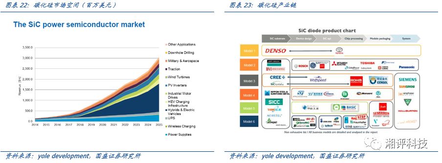
The industrialization of SiC is accelerating, with upstream supply chains beginning to expand and secure sources. According to CREE announcements, the recent pace of SiC industrialization has started to accelerate, with midstream manufacturers like ST and Infineon starting to secure upstream wafer supplies:
➤ In January 2019, CREE announced a multi-year production supply agreement worth $250 million with ST, whereby Wolfspeed will supply 150mm SiC wafers to ST.
➤ In October 2018, CREE announced a long-term agreement worth $85 million to produce and supply SiC wafers for a leading power equipment company whose name has not been disclosed.
➤ In February 2018, CREE signed a $100 million long-term supply agreement with Infineon to provide SiC wafers for products such as photovoltaic inverters, robotics, charging infrastructure, industrial power supplies, traction, and variable speed drives.
Overseas Commercialization Leads, Strong Expectations for 5G Acceleration
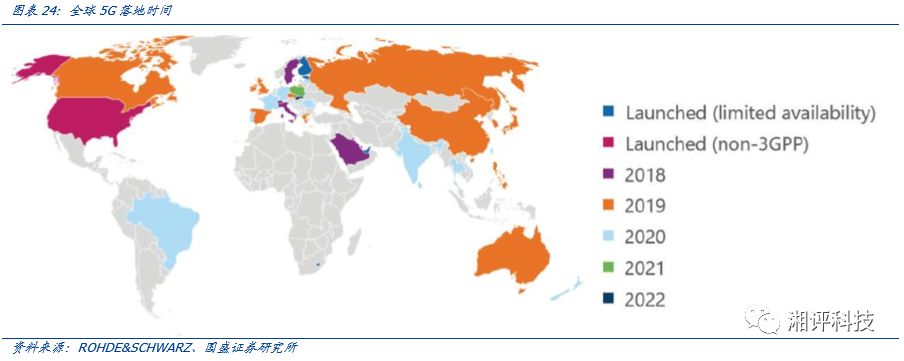
Overseas 5G commercialization is leading, and domestic 5G advancement is expected to accelerate! On April 3, American operator Verizon announced the launch of 5G services in certain areas; on April 5, South Korea’s three major operators announced the start of 5G commercial services for ordinary consumers; on April 10, the Japanese government allocated 5G frequency bands to four major operators, with formal commercialization expected next spring; we believe that with the active pace of overseas 5G commercialization, domestic 5G is expected to accelerate.
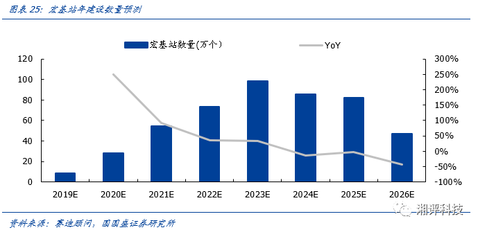
With the promotion of 5G, from the construction demand of 5G, a “macro station plus small station” network coverage model will be adopted. Each upgrade of base stations will lead to a wave of renovations of existing base stations and the construction of new base stations. By 2017, the 4G coverage phase in China was basically completed, with 3.28 million macro base stations reaching. According to predictions from CCID Consulting, the total number of 5G macro base stations will be 1.1 to 1.5 times that of 4G macro base stations, corresponding to 3.6 million to 4.92 million 5G macro base stations.
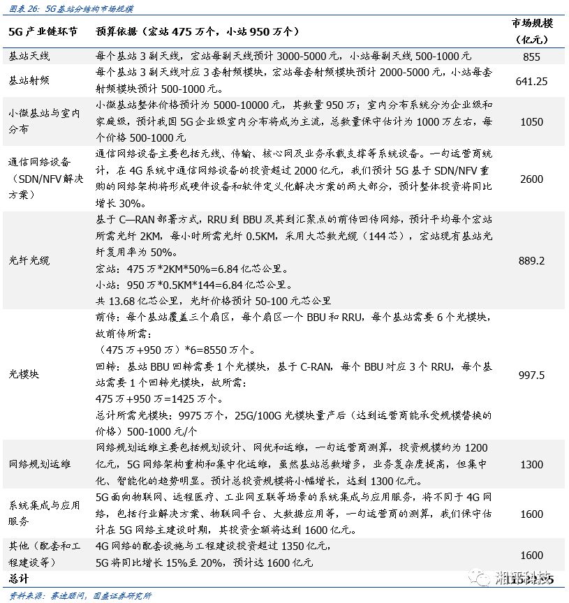
At the same time, for small stations, the coverage range of millimeter-wave high-frequency bands is 10-20m, applied in hotspot areas or scenarios with higher capacity demands, and their number is conservatively estimated to be twice that of macro stations, leading us to expect that there will be 9.5 million 5G small stations.
Base station construction will be one of the main driving forces for the growth of the gallium nitride market. Yole Development data shows that in 2018, the gallium nitride RF device market size at the base station end was less than $200 million, and it is expected that by 2023, the gallium nitride market size at the base station end will exceed $500 million. The overall gallium nitride RF device market will maintain a compound annual growth rate of 23%, with the market size expected to reach $1.3 billion by 2023.
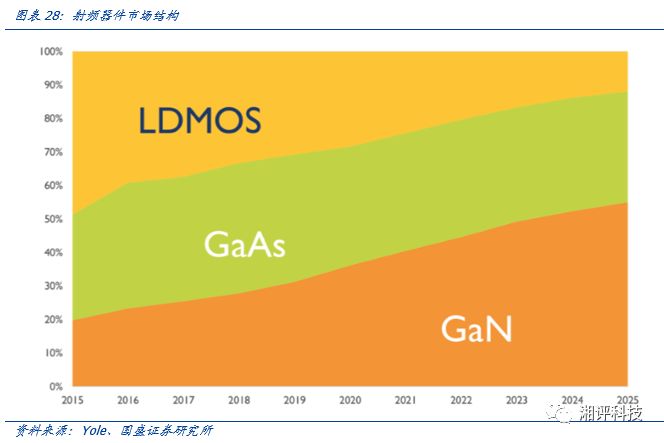
Gallium nitride will hold half of the RF device market. In the RF device field, currently, LDMOS (Lateral Diffused Metal Oxide Semiconductor), GaAs (Gallium Arsenide), and GaN (Gallium Nitride) have similar market shares, but according to Yole Development’s forecast, by 2025, while the market share of gallium arsenide remains relatively stable, gallium nitride is expected to replace a significant portion of LDMOS share, occupying about 50% of the RF device market.
Electrification of Automobiles Drives Rapid Growth in Silicon Carbide Market
Rapid Growth in the Automotive Semiconductor Market
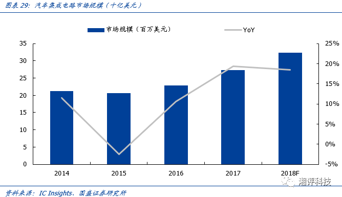
The automotive IC market is growing rapidly, becoming a highlight of semiconductor growth. According to IC Insights data, the automotive IC market is expected to grow by 18.5% in 2018, reaching a scale of $32.3 billion. By 2021, the automotive IC market will grow to $43.6 billion, with a compound annual growth rate of 12.5% between 2017 and 2021, making it the highest compound growth rate among sub-markets, and one of the main driving forces for the future.
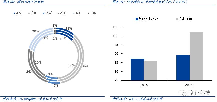
Strong Growth in Automotive Analog ICs, Surpassing Smartphones. The rapid growth of smartphones was once the main driving force behind the growth of the semiconductor market, but now automobiles have become the next contender. According to HIS data, in terms of volume, the automotive analog IC market is expected to surpass the smartphone market by 2015, reaching $10.2 billion by 2018. Meanwhile, as the automotive market grows faster than other sub-industries, its share of analog IC sales also increases year by year.
Environmental and energy-saving demands are driving the electrification of automobiles, leading to rapid growth in new energy vehicles. Due to the high importance placed by governments on energy and environmental issues, many have proposed plans to ban the sale of fuel vehicles, making the electrification of automobiles an inevitable trend. According to Katusa Research data, China, the United States, and Germany will become the main promoters of electric vehicles, leading to an average annual sales volume of 6 million electric vehicles by 2040. New energy vehicles can effectively reduce fuel consumption, and they require a large number of power ICs (such as DC/DC converters for voltage regulation), benefiting the analog IC industry.
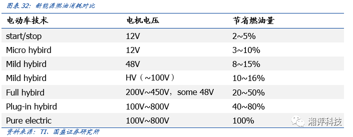
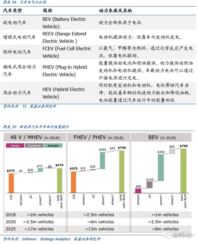
The electrification of automobiles is deepening, and the value of silicon continues to grow. Automakers are launching new energy vehicles to achieve a soft replacement for automobile electrification. Common new energy vehicles include hybrid electric vehicles, plug-in hybrid vehicles, extended-range electric vehicles, and pure electric vehicles. As the degree of electrification increases, the semiconductor value of automobiles is also rising. In 2018, the semiconductor value per vehicle for moderate hybrid vehicles, plug-in hybrid vehicles, and pure electric vehicles reached $475, $740, and $750, respectively. According to Strategy Analytics, by 2025, the sales volume of hybrid vehicles, plug-in hybrid vehicles, and pure electric vehicles is expected to reach 17 million, 13 million, and 8 million, respectively, with a total semiconductor market size reaching $23.7 billion.
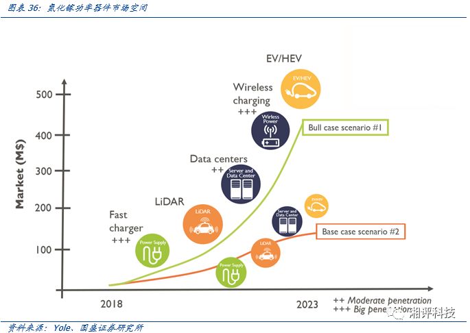
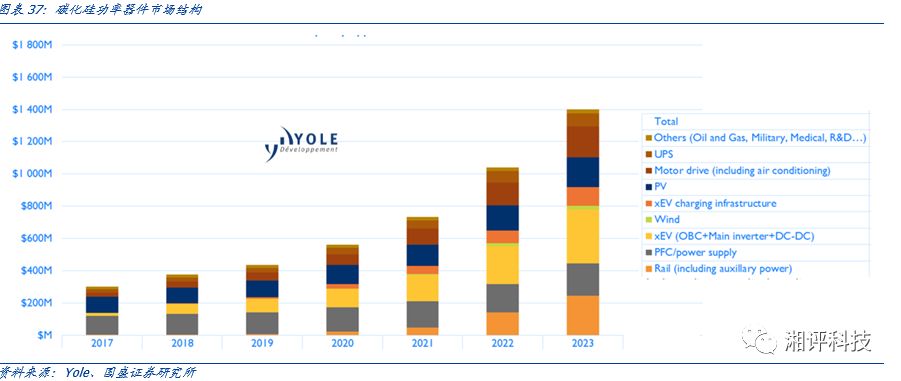
The electric vehicle market will be the main driver for the growth of silicon carbide devices. According to Yole Development, in the coming years, new energy vehicles, motor drives, and railways will significantly impact the growth of the silicon carbide market, with the highest incremental value coming from new energy vehicles, including the vehicles themselves and various infrastructure construction driven by them.
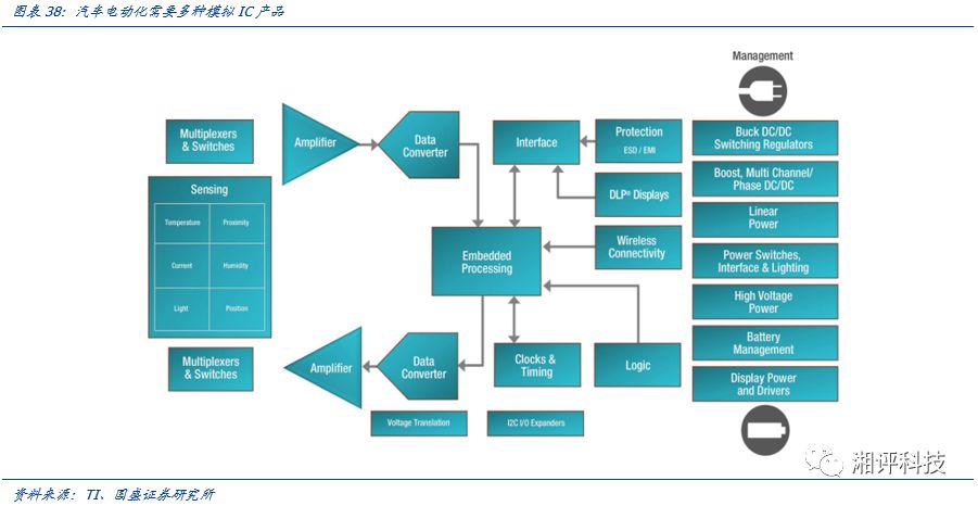
Automobiles, for safety considerations, require various subsystems for voltage regulation, electrostatic protection, signal isolation, etc., and also need many power semiconductor products that are compatible with power systems, including chargers, battery management systems, inverters, sub-inverters, DC/DC converters, and various interfaces. Therefore, the electrification of automobiles provides a broader market space for power semiconductors.
(Source: Today’s Semiconductor. This article is produced by the Qingdao West Coast International Investment Promotion Center, and is reproduced only for sharing and learning, not for commercial use. If there is any infringement, please contact us for removal.)