
Click the blue text
Follow us
STM32 SPI Communication
-
High-speed full-duplex communication bus
The SPI communication uses 3 lines and a chip select line. The 3 lines are SCK, MOSI, and MISO, and the chip select line is NSS (CS).
-
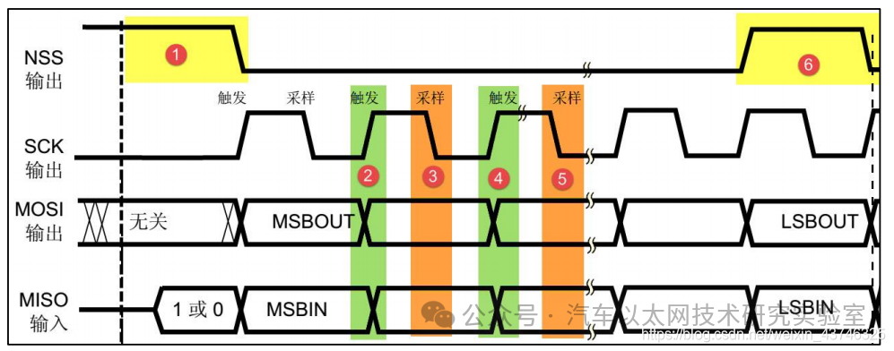
The NSS signal line goes from high to low, which is the start signal for SPI communication. NSS is a signal line that is exclusively owned by each slave. When a slave detects the start signal on its own NSS line, it knows it has been selected by the master and begins to prepare for communication with the master. In the diagram, at the marked point , the NSS signal goes from low to high, which is the stop signal for SPI communication, indicating that the communication has ended and the slave’s selected state is canceled.
-
SPI uses the MOSI and MISO signal lines to transmit data, and the SCK signal line for data synchronization. The MOSI and MISO data lines transmit one bit of data on each clock cycle of SCK, and data input and output occur simultaneously.
-
There are four communication modes in SPI, and their main differences lie in the clock state of SCK when the bus is idle and the timing of data sampling. To facilitate explanation, we introduce the concepts of “Clock Polarity (CPOL)” and “Clock Phase (CPHA).”
-
Clock Polarity (CPOL) refers to the level signal of the SCK line when the SPI communication device is in an idle state (i.e., the state of SCK before SPI communication starts, when the NSS line is high). When CPOL=0, SCK is low in idle state; when CPOL=1, it is the opposite.
-
Clock Phase (CPHA) refers to the timing of data sampling. When CPHA=0, the signal on the MOSI or MISO data line will be sampled on the “odd edge” of the SCK clock line. When CPHA=1, the data line is sampled on the “even edge” of SCK.
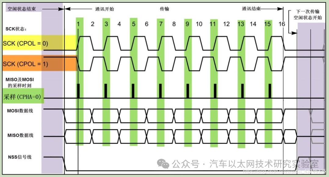
SPI communication mode when CPHA=0
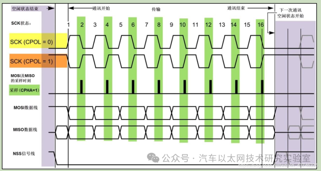
SPI communication mode when CPHA=1:
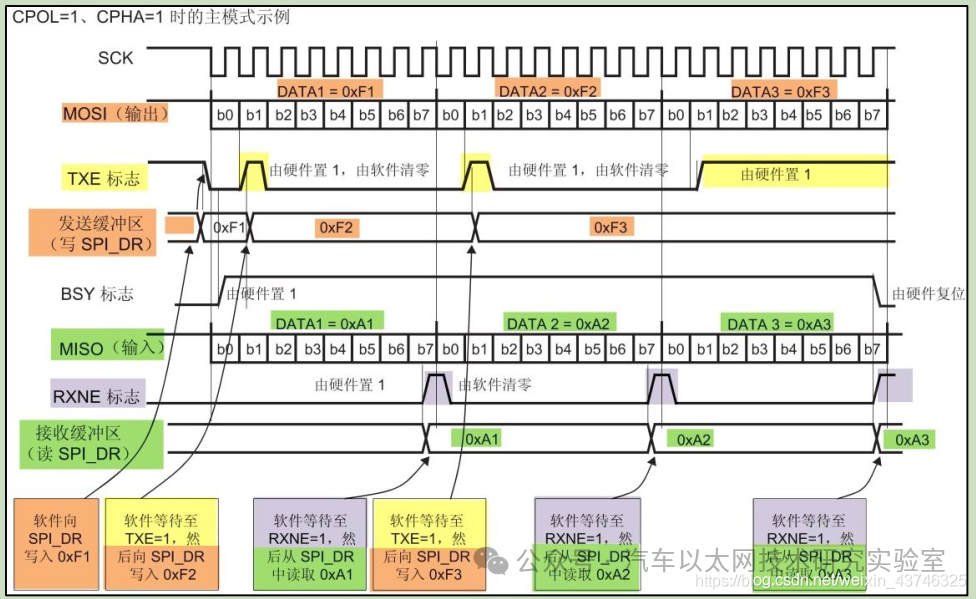
1. First, pull the chip select line NSS low,
2. Write data into the transmission buffer, the SCK clock starts running, and MOSI will automatically send the data from the transmission buffer. After sending a frame of data, when the transmission buffer is empty, the TXE flag will change to 1, allowing further data to be sent.
3. By checking whether the receive buffer flag is 1 (the receive buffer is not empty), read the data from the receive buffer.
-
The SCLK signal line is controlled only by the master device; the slave device cannot control the signal line. Similarly, in an SPI-based device, there must be at least one master device;
-
In point-to-point communication, the SPI interface does not require addressing operations and is full-duplex communication, making it simple and efficient. In a system with multiple slave devices, each slave device requires an independent enable signal, making the hardware slightly more complex than an I2C system.
Is it MSB first (most significant bit first) or LSB first (least significant bit first)?
From the bit perspective, MSB in the SPI protocol indicates that the high bit is sent first. Similarly, LSB indicates that the low bit is sent first. This should not be confused with endianness.
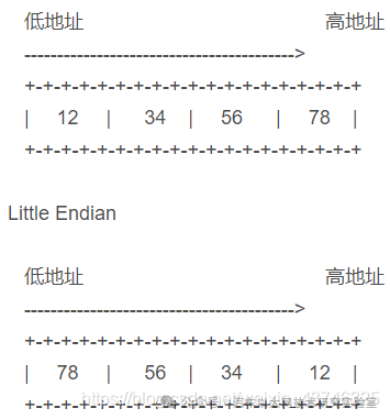
Endianness issue (from the byte perspective)
Big endian means that the most significant byte is stored at the lowest address (big endian, high byte at low address), while little endian means that the least significant byte is stored at the lowest address (little endian, low byte at low address).
For example, with 0x12345678, the storage order in two different byte order CPUs is as follows:
SPI_DEMO Practice
STM32 Master-Slave Dual Machine SPI Communication Test:
Functionality: Master and slave devices can receive data from each other

Wiring:
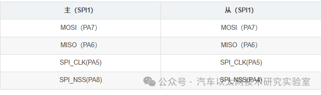
The connections are one-to-one; do not connect MOSI to MISO, and the configuration parameters of both devices such as rate, phase, polarity, CRC, transmission direction, and bit count must be the same. Remember, they must share a common ground.
Main code for the master device:
-
/* Master device stm32f103c8 SPI1 */
-
int main(void)
-
{
-
u16 t;
-
u8 send_data=’A’;
-
u8 led_flag = 0;
-
delay_init(); // Delay function initialization
-
NVIC_PriorityGroupConfig(NVIC_PriorityGroup_2); // Set NVIC interrupt group 2: 2 bits preemptive priority, 2 bits response priority
-
uart_init(115200); // UART initialization to 115200
-
LED_Init(); // LED port initialization
-
KEY_Init(); // Key PB9 pull-up to detect low level
-
spi_M_init(); // SPI1
-
SPI_MCU_CS_LOW(); // Start signal low level selected to communicate with the slave device
-
while(1)
-
{
-
if(KEY0==0)
-
{
-
delay_ms(5);
-
if(KEY0==0){
-
/* Check if the specified SPI flag is set: transmission buffer empty flag, no data */
-
while (SPI_I2S_GetFlagStatus(MCU_SPIx, SPI_I2S_FLAG_TXE) == RESET); // Check if the specified SPI flag is set: transmission buffer empty flag
-
SPI_I2S_SendData(MCU_SPIx, send_data); // Send a data through peripheral SPIx
-
/* Wait for one byte to be received */
-
while (SPI_I2S_GetFlagStatus(MCU_SPIx, SPI_I2S_FLAG_RXNE) == RESET);
-
/* Send the data sent by the slave device, which is the data received by the master device, to the UART transmission buffer */
-
USART1->DR = SPI_I2S_ReceiveData(MCU_SPIx);
-
led_flag++;
-
send_data++;}
-
while(KEY0==0);
-
}else{
-
}
-
if(led_flag%2)
-
GPIO_SetBits(GPIOC,GPIO_Pin_13);
-
else
-
GPIO_ResetBits(GPIOC,GPIO_Pin_13);
-
}
-
}
-
// SPI master mode configuration
-
void spi_M_init(void){
-
SPI_InitTypeDef SPI_InitStructure;
-
GPIO_InitTypeDef GPIO_InitStructure;
-
NVIC_InitTypeDef NVIC_InitStructure;
-
/* Enable SPI clock */
-
MCU_SPI_APBxClock_FUN ( MCU_SPI_CLK, ENABLE );
-
/* Enable clock for SPI related pins */
-
MCU_SPI_CS_APBxClock_FUN ( MCU_SPI_CS_CLK|MCU_SPI_SCK_CLK|MCU_SPI_MISO_PIN|MCU_SPI_MOSI_PIN, ENABLE );
-
/* Configure the CS pin of SPI, it can be a normal IO */
-
GPIO_InitStructure.GPIO_Pin = MCU_SPI_CS_PIN;
-
GPIO_InitStructure.GPIO_Speed = GPIO_Speed_50MHz;
-
GPIO_InitStructure.GPIO_Mode = GPIO_Mode_Out_PP;
-
GPIO_Init(MCU_SPI_CS_PORT, &GPIO_InitStructure);
-
/* Configure the SCK pin of SPI */
-
GPIO_InitStructure.GPIO_Pin = MCU_SPI_SCK_PIN;
-
GPIO_InitStructure.GPIO_Mode = GPIO_Mode_AF_PP;
-
GPIO_Init(MCU_SPI_SCK_PORT, &GPIO_InitStructure);
-
/* Configure the MISO pin of SPI */
-
GPIO_InitStructure.GPIO_Pin = MCU_SPI_MISO_PIN;
-
GPIO_Init(MCU_SPI_MISO_PORT, &GPIO_InitStructure);
-
/* Configure the MOSI pin of SPI */
-
GPIO_InitStructure.GPIO_Pin = MCU_SPI_MOSI_PIN;
-
GPIO_Init(MCU_SPI_MOSI_PORT, &GPIO_InitStructure);
-
/* Stop signal MCU: CS pin high level */
-
SPI_MCU_CS_HIGH();
-
/* SPI mode configuration */
-
// MCU chip supports SPI mode 0 and mode 3, set CPOL CPHA accordingly
-
SPI_InitStructure.SPI_Direction = SPI_Direction_2Lines_FullDuplex;
-
SPI_InitStructure.SPI_Mode = SPI_Mode_Master;
-
SPI_InitStructure.SPI_DataSize = SPI_DataSize_8b;
-
SPI_InitStructure.SPI_CPOL = SPI_CPOL_High;
-
SPI_InitStructure.SPI_CPHA = SPI_CPHA_2Edge;
-
SPI_InitStructure.SPI_NSS = SPI_NSS_Soft;// Note this
-
SPI_InitStructure.SPI_BaudRatePrescaler = SPI_BaudRatePrescaler_256;//
-
SPI_InitStructure.SPI_FirstBit = SPI_FirstBit_MSB;
-
SPI_InitStructure.SPI_CRCPolynomial = 7;
-
SPI_Init(MCU_SPIx , &SPI_InitStructure);
-
/* Enable SPI */
-
SPI_Cmd(MCU_SPIx , ENABLE);
-
//SPI_I2S_ITConfig(MCU_SPIx, SPI_I2S_IT_RXNE, ENABLE); // Enable receive interrupt
-
/* NVIC interrupt controller configuration */
-
// NVIC_PriorityGroupConfig(NVIC_PriorityGroup_2); // Interrupt priority group 2
-
// NVIC_InitStructure.NVIC_IRQChannel = SPI1_IRQn; // SPI2 interrupt
-
// NVIC_InitStructure.NVIC_IRQChannelPreemptionPriority=1; // Preemptive priority 3
-
// NVIC_InitStructure.NVIC_IRQChannelSubPriority =3; // Sub-priority 3
-
// NVIC_InitStructure.NVIC_IRQChannelCmd = ENABLE; // Enable IRQ channel
-
// NVIC_Init(&NVIC_InitStructure); // Initialize VIC register according to specified parameters
-
}
Main code for the slave device:
-
To allow the master to initially receive valid data, first store the data to be sent in the transmission buffer SPI_I2S_SendData(MCU_SPIx,‘n’);. One point to note is that at this time, the data has not yet been sent to the master device, as the slave device cannot actively send data but must passively send data, waiting for the master device to send data, which means it must wait for a clock signal cycle. When the slave device receives the clock signal (CLK), it moves the data from the transmission buffer to the shift register and sends it to the master device.
-
Since it is a slave device, the SPI1 chip select pin will be reused, hardware chip select.
-
//stm32f103c8 Slave device
-
int main(void)
-
{
-
u16 retry;
-
u8 send_data=’a’;
-
u8 led_flag=0;
-
delay_init(); // Delay function initialization
-
NVIC_PriorityGroupConfig(NVIC_PriorityGroup_2); // Set NVIC interrupt group 2: 2 bits preemptive priority, 2 bits response priority
-
uart_init(115200); // UART initialization to 115200
-
LED_Init(); // LED port initialization
-
KEY_Init();
-
spi_S_init();
-
while (SPI_I2S_GetFlagStatus(MCU_SPIx, SPI_I2S_FLAG_TXE) == RESET); // Check if the specified SPI flag is set: receive buffer non-empty flag
-
SPI_I2S_SendData(MCU_SPIx,’n’);//
-
while(1)
-
{
-
// while (SPI_I2S_GetFlagStatus(MCU_SPIx, SPI_I2S_FLAG_TXE) == RESET); // Check if the specified SPI flag is set: receive buffer non-empty flag
-
// SPI_I2S_SendData(MCU_SPIx,’n’);
-
}
-
}
-
// SPI slave mode configuration
-
void spi_S_init(void){
-
SPI_InitTypeDef SPI_InitStructure;
-
GPIO_InitTypeDef GPIO_InitStructure;
-
NVIC_InitTypeDef NVIC_InitStructure;
-
/* Enable SPI clock */
-
MCU_SPI_APBxClock_FUN ( MCU_SPI_CLK, ENABLE );
-
/* Enable clock for SPI related pins */
-
MCU_SPI_CS_APBxClock_FUN ( MCU_SPI_CS_CLK|MCU_SPI_SCK_CLK|MCU_SPI_MISO_PIN|MCU_SPI_MOSI_PIN, ENABLE );
-
/* Configure the CS pin of SPI, it can be a normal IO */
-
GPIO_InitStructure.GPIO_Pin = MCU_SPI_CS_PIN;
-
// GPIO_InitStructure.GPIO_Speed = GPIO_Speed_50MHz;
-
GPIO_InitStructure.GPIO_Mode = GPIO_Mode_AF_PP;
-
GPIO_Init(MCU_SPI_CS_PORT, &GPIO_InitStructure);
-
/* Configure the SCK pin of SPI */
-
GPIO_InitStructure.GPIO_Pin = MCU_SPI_SCK_PIN;
-
GPIO_InitStructure.GPIO_Mode = GPIO_Mode_AF_PP;
-
GPIO_Init(MCU_SPI_SCK_PORT, &GPIO_InitStructure);
-
/* Configure the MISO pin of SPI */
-
GPIO_InitStructure.GPIO_Pin = MCU_SPI_MISO_PIN;
-
GPIO_Init(MCU_SPI_MISO_PORT, &GPIO_InitStructure);
-
/* Configure the MOSI pin of SPI */
-
GPIO_InitStructure.GPIO_Pin = MCU_SPI_MOSI_PIN;
-
GPIO_Init(MCU_SPI_MOSI_PORT, &GPIO_InitStructure);
-
/* Stop signal MCU: CS pin high level */
-
// SPI_MCU_CS_HIGH();
-
/* SPI mode configuration */
-
// MCU chip supports SPI mode 0 and mode 3, set CPOL CPHA accordingly
-
SPI_InitStructure.SPI_Direction = SPI_Direction_2Lines_FullDuplex;
-
SPI_InitStructure.SPI_Mode = SPI_Mode_Slave;
-
SPI_InitStructure.SPI_DataSize = SPI_DataSize_8b;
-
SPI_InitStructure.SPI_CPOL = SPI_CPOL_High;
-
SPI_InitStructure.SPI_CPHA = SPI_CPHA_2Edge;
-
SPI_InitStructure.SPI_NSS = SPI_NSS_Hard;// As a slave, chip select
-
SPI_InitStructure.SPI_BaudRatePrescaler = SPI_BaudRatePrescaler_256;
-
SPI_InitStructure.SPI_FirstBit = SPI_FirstBit_MSB;
-
SPI_InitStructure.SPI_CRCPolynomial = 7;
-
SPI_Init(MCU_SPIx , &SPI_InitStructure);
-
/* Enable SPI */
-
SPI_Cmd(MCU_SPIx , ENABLE);
-
SPI_I2S_ITConfig(MCU_SPIx, SPI_I2S_IT_RXNE, ENABLE); // Enable receive interrupt
-
NVIC_InitStructure.NVIC_IRQChannel = SPIX_IRQ; // SPI1 interrupt
-
NVIC_InitStructure.NVIC_IRQChannelPreemptionPriority=1; // Preemptive priority 3
-
NVIC_InitStructure.NVIC_IRQChannelSubPriority =3; // Sub-priority 3
-
NVIC_InitStructure.NVIC_IRQChannelCmd = ENABLE; // Enable IRQ channel
-
NVIC_Init(&NVIC_InitStructure); // Initialize VIC register according to specified parameters
-
}
-
u8 send_data=’a’;
-
u8 led_flag=0;
-
// Interrupt handling function
-
void handle_spi_fun(void)
-
{
-
/* Check if the receive buffer is non-empty */
-
if (SET == SPI_I2S_GetITStatus(MCU_SPIx, SPI_I2S_IT_RXNE))
-
{
-
USART1->DR = MCU_SPIx->DR; /* Read data from the receive buffer */
-
while (SPI_I2S_GetFlagStatus(MCU_SPIx, SPI_I2S_FLAG_TXE) == RESET);
-
MCU_SPIx->DR = send_data;
-
if(led_flag%2)
-
GPIO_ResetBits(GPIOC,GPIO_Pin_13);
-
else
-
GPIO_SetBits(GPIOC,GPIO_Pin_13);
-
led_flag++;
-
send_data++;
-
/* Clear interrupt flag */
-
SPI_I2S_ClearITPendingBit(MCU_SPIx, SPI_I2S_IT_RXNE);
-
}
-
}
Test results:
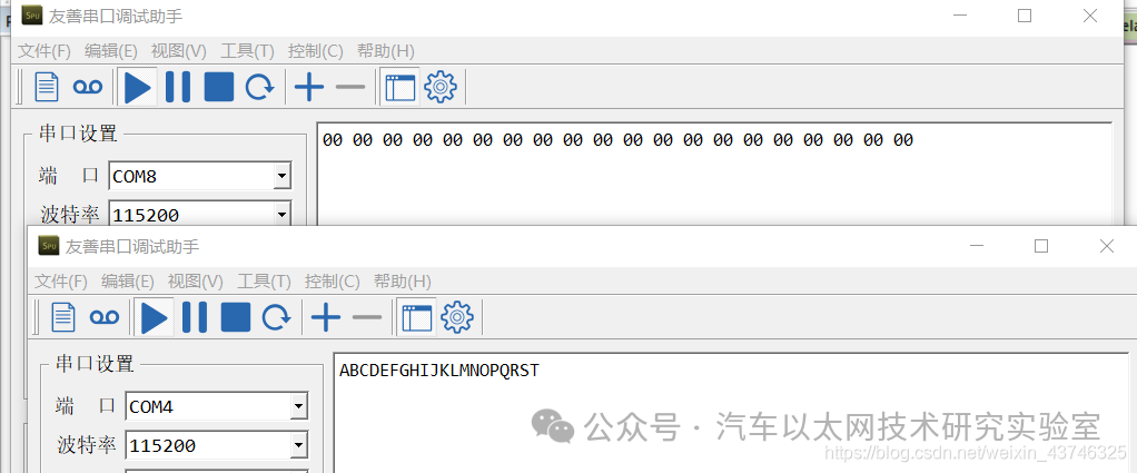
COM8 is the master device receiving data from the slave device, and COM4 is the slave device receiving data from the master device.
It is evident that the master device failed to successfully obtain data from the slave device, while the slave device received data from the master device.
Problem analysis:
1. The problem lies with the master device: the master device did not receive or respond.
2. The problem lies with the slave device: the slave device did not send data.
3. Both of the above problems occurred simultaneously.
Connection issues:
1. First, I connected the master device’s MOSI to its own MISO, and the test result showed that the master device could receive data. This ruled out the first possibility.
2. During communication between the master and slave devices, I used a logic analyzer to detect the MISO pin and did not detect any waveform changes. The problem is likely with the slave device.
So, I replaced the slave device with STM32F429, while the master device remained STM32F103C8, and the program remained the same.

Wiring:
-
/*stm32F429IG SPI2 Slave device*/
-
#define SELECT_MASTER 0
-
int main(void)
-
{
-
u8 send_data=’a’;
-
u8 led_flag=0;
-
LED_GPIO_Config();//PB0 PB1
-
Debug_USART_Config();// UART1 115200
-
SPI_MCU_Init();// SPI2
-
key_init();// PA0 Key
-
#if SELECT_MASTER // Set in bsp_spi_mcu.h file
-
send_data=’A’;
-
#else
-
/* Check if the transmission buffer is empty, a point to note
-
As a slave device, placing data in the transmission buffer does not mean it has been sent to the master device,
-
It must wait for the master device to send data, which means it needs a clock signal (SCK)
-
*/
-
while (SPI_I2S_GetFlagStatus(MCU_SPI, SPI_I2S_FLAG_TXE) == RESET);
-
/* Write data to the data register, writing the data to the transmission buffer */
-
SPI_I2S_SendData(MCU_SPI, send_data);
-
#endif
-
while(1){
-
// Master device
-
#if SELECT_MASTER // Set in bsp_spi_mcu.h file
-
if(KEY==1)
-
{
-
delay(0x0F);
-
if(KEY==1){
-
/* Check if the transmission buffer is empty, no data */
-
while (SPI_I2S_GetFlagStatus(MCU_SPI, SPI_I2S_FLAG_TXE) == RESET);
-
/* Write data to the data register, writing the data to the transmission buffer */
-
SPI_I2S_SendData(MCU_SPI, send_data);
-
/* Check if the receive buffer is non-empty, there is data */
-
while (SPI_I2S_GetFlagStatus(MCU_SPI, SPI_I2S_FLAG_RXNE) == RESET);
-
/* Send the received data to the UART transmission buffer */
-
USART1->DR = SPI_I2S_ReceiveData(MCU_SPI);
-
led_flag++;
-
send_data++;
-
while(KEY==1);
-
}else{}
-
}
-
#else
-
// Slave device
-
/* Check if the receive buffer is non-empty, there is data */
-
while(SPI_I2S_GetFlagStatus(MCU_SPI, SPI_I2S_FLAG_RXNE) == RESET);
-
/* Send the received data to the UART transmission buffer */
-
USART1->DR = SPI_I2S_ReceiveData(MCU_SPI);
-
/* Check if the transmission buffer is empty, no data */
-
while (SPI_I2S_GetFlagStatus(MCU_SPI, SPI_I2S_FLAG_TXE) == RESET);
-
/* Write data to the data register, writing the data to the transmission buffer */
-
SPI_I2S_SendData(MCU_SPI, send_data);
-
led_flag++;
-
send_data++;
-
#endif
-
// Each time the slave device sends data or the master device presses a key, LED1 PB0 toggles
-
if(led_flag%2)
-
LED1_OFF
-
else
-
LED1_ON
-
}
-
}
-
// SPI2 configuration
-
void SPI_MCU_Init(void)
-
{
-
SPI_InitTypeDef SPI_InitStructure;
-
GPIO_InitTypeDef GPIO_InitStructure;
-
/* Enable MCU_SPI and GPIO clock */
-
/*!< Enable clock for SPI_MCU_SPI_CS_GPIO, SPI_MCU_SPI_MOSI_GPIO,
-
SPI_MCU_SPI_MISO_GPIO,SPI_MCU_SPI_SCK_GPIO */
-
RCC_AHB1PeriphClockCmd (MCU_SPI_SCK_GPIO_CLK | MCU_SPI_MISO_GPIO_CLK|MCU_SPI_MOSI_GPIO_CLK|MCU_CS_GPIO_CLK, ENABLE);
-
/*!< Enable clock for SPI_MCU_SPI */
-
MCU_SPI_CLK_INIT(MCU_SPI_CLK, ENABLE);
-
// Set pin multiplexing
-
GPIO_PinAFConfig(MCU_SPI_SCK_GPIO_PORT,MCU_SPI_SCK_PINSOURCE,MCU_SPI_SCK_AF);
-
GPIO_PinAFConfig(MCU_SPI_MISO_GPIO_PORT,MCU_SPI_MISO_PINSOURCE,MCU_SPI_MISO_AF);
-
GPIO_PinAFConfig(MCU_SPI_MOSI_GPIO_PORT,MCU_SPI_MOSI_PINSOURCE,MCU_SPI_MOSI_AF);
-
/*!< Configure SPI_MCU_SPI pin: SCK */
-
GPIO_InitStructure.GPIO_Pin = MCU_SPI_SCK_PIN;
-
GPIO_InitStructure.GPIO_Speed = GPIO_Speed_50MHz;
-
GPIO_InitStructure.GPIO_Mode = GPIO_Mode_AF;
-
GPIO_InitStructure.GPIO_OType = GPIO_OType_PP;
-
GPIO_InitStructure.GPIO_PuPd = GPIO_PuPd_NOPULL;
-
GPIO_Init(MCU_SPI_SCK_GPIO_PORT, &GPIO_InitStructure);
-
/*!< Configure SPI_MCU_SPI pin: MISO */
-
GPIO_InitStructure.GPIO_Pin = MCU_SPI_MISO_PIN;
-
GPIO_Init(MCU_SPI_MISO_GPIO_PORT, &GPIO_InitStructure);
-
/*!< Configure SPI_MCU_SPI pin: MOSI */
-
GPIO_InitStructure.GPIO_Pin = MCU_SPI_MOSI_PIN;
-
GPIO_Init(MCU_SPI_MOSI_GPIO_PORT, &GPIO_InitStructure);
-
/*!< Configure SPI_MCU_SPI pin: CS */
-
GPIO_InitStructure.GPIO_Pin = MCU_CS_PIN;
-
#if SELECT_MASTER
-
GPIO_InitStructure.GPIO_Mode = GPIO_Mode_OUT;
-
#else
-
/* As a slave device, the hardware chip select pin CS needs to be multiplexed */
-
GPIO_PinAFConfig(MCU_CS_GPIO_PORT,MCU_SPI_CS_PINSOURCE,MCU_SPI_CS_AF);
-
#endif
-
GPIO_Init(MCU_CS_GPIO_PORT, &GPIO_InitStructure);
-
/* Stop signal MCU: CS pin high level */
-
// SPI_MCU_CS_HIGH();
-
/* MCU_SPI mode configuration */
-
// MCU chip supports SPI mode 0 and mode 3, set CPOL CPHA accordingly
-
SPI_InitStructure.SPI_Direction = SPI_Direction_2Lines_FullDuplex;
-
#if SELECT_MASTER
-
SPI_InitStructure.SPI_Mode = SPI_Mode_Master;
-
SPI_InitStructure.SPI_NSS = SPI_NSS_Soft;
-
#else
-
/* Slave mode, set hardware chip select */
-
SPI_InitStructure.SPI_Mode = SPI_Mode_Slave;
-
SPI_InitStructure.SPI_NSS = SPI_NSS_Hard;
-
#endif
-
SPI_InitStructure.SPI_DataSize = SPI_DataSize_8b;
-
SPI_InitStructure.SPI_CPOL = SPI_CPOL_High;
-
SPI_InitStructure.SPI_CPHA = SPI_CPHA_2Edge;
-
SPI_InitStructure.SPI_BaudRatePrescaler = SPI_BaudRatePrescaler_256;
-
SPI_InitStructure.SPI_FirstBit = SPI_FirstBit_MSB;
-
SPI_InitStructure.SPI_CRCPolynomial = 7;
-
SPI_Init(MCU_SPI, &SPI_InitStructure);
-
/* Enable MCU_SPI */
-
SPI_Cmd(MCU_SPI, ENABLE);
-
}
-

Results:
COM8 is the master device receiving data from the slave device, and COM1 is the slave device receiving data from the master device.
The output results from the serial port indicate that the test was successful.
To further validate my hypothesis, I swapped the master and slave modes of STM32F1 and STM32F4, and the result was the same: the master device (F4) failed to successfully receive data sent by the slave device (F1), while the slave device could receive data.
Conclusion:
When STM32F103 is used as a slave, it can receive data but cannot send data or experiences data shifting issues.
Additionally: The two microcontrollers have different clock frequencies; F4 has a clock frequency of 180MHz, while F1 has a clock frequency of 72MHz. The APB2 clock frequency for F4 is 90MHz, and the APB1 clock frequency is 45MHz; for F1, the APB2 clock frequency is 72MHz, and the APB1 clock frequency is 36MHz. The SPI1 device is a high-speed device belonging to the APB2 bus, while SPI2 is a low-speed device belonging to the APB1 bus. Therefore, under the same configuration parameters, for example, when SPI1 is the master, the SCLK clock frequency is 72MHz/256=2812.5 KHz, while SPI2 is 36MHz/256=140.625 KHz.


*Disclaimer: This article is original or forwarded by the author. If it inadvertently infringes on someone’s intellectual property, please inform us for deletion.The above images and text are sourced from the internet. If there is any infringement, please contact us in a timely manner, and we will delete it within 24 hours.The content of the article reflects the author’s personal views, and the Automotive Ethernet Technology Research Laboratory reprints it only to convey a different perspective, which does not represent the Automotive Ethernet Technology Research Laboratory’s endorsement or support of this view. If there are any objections, please contact the Automotive Ethernet Technology Research Laboratory.
Original link:
https://blog.csdn.net/weixin_43746325/article/details/119545607