Introduction
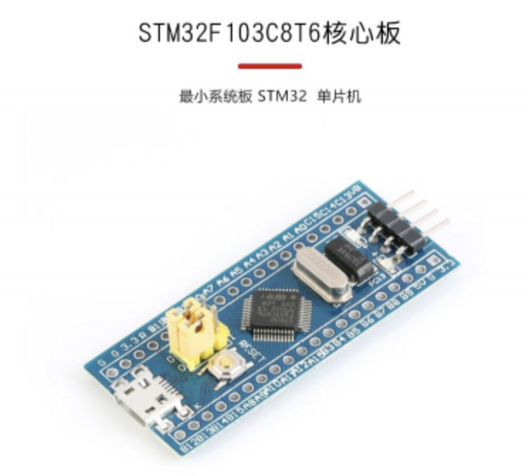
The car parking lock system based on RFID video technology consists of a core circuit board with STM32F103C8T6 microcontroller, an LCD1602 liquid crystal display circuit, an RFID module circuit, a button circuit, and a relay circuit.
The relay simulates the car parking entrance lock switch, normally closed to prevent other vehicles from entering. If the card is successfully swiped, the relay opens, allowing the vehicle to enter.
Learning: Focus on using the RC552 RFID radio frequency module, primarily learning to use the RC552 RFID radio frequency module.
Design Background and Significance
Radio Frequency Identification (RFID) technology, also known as wireless radio frequency identification, is a communication technology that can identify specific targets and read/write related data through radio signals without mechanical or optical contact between the identification system and the specific target.
RFID technology has advantages such as waterproof, anti-magnetic, high-temperature resistance, long lifespan, large reading distance, encrypted data on tags, larger data storage capacity, and flexible information modification, making it applicable in various fields. The rapid economic development has led to increasing concern for the security of buildings.
To meet the needs of the information age and ensure the security of buildings, intelligent access control systems have been developed.
The access control system integrates computer technology, electronic technology, mechanical technology, magnetic technology, and radio frequency identification technology to control the unlocking of doors using smart cards. It not only provides managers with a safer, faster, and more automated management model but also brings great convenience to users.
Design and Verification of the Solution
Determination of Control Scheme
The system is composed of STM32F103C8T6 microcontroller core circuit, LCD1602 liquid crystal display circuit, RFID module circuit, button circuit, and relay circuit.
Selection of Control Method
The STM32 microcontroller is chosen; the STM32 series processors are 32-bit microcontrollers based on the ARM 7 architecture produced by STMicroelectronics, supporting real-time simulation and tracing.
Using the latest advanced architecture Cortex-M3 core from ARM, it has excellent real-time performance, outstanding power control, remarkable and innovative peripherals, and maximally integrated design, making it very easy to develop and allowing products to quickly enter the market.
Hardware Circuit Design
System Function Analysis and Architecture Design
System function analysis
The relay simulates the car parking entrance lock switch (similar to the car parking post in front), normally closed to prevent other vehicles from entering. If the card is successfully swiped, the relay opens, allowing the vehicle to enter.
After the vehicle enters, the relay can be opened again through the button, unlocking the parking post to secure the vehicle in place.
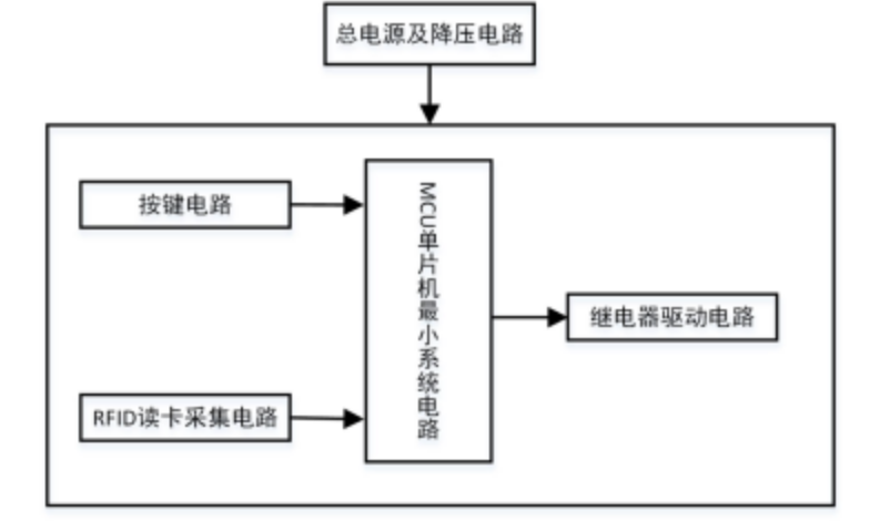
Overall Structure of the System
The specific block diagram of this system is shown below:
STM32 Microcontroller Core Circuit Design
The STM32 series processors are 32-bit microcontrollers based on the ARM 7 architecture produced by STMicroelectronics.
This control chip is chosen because the design of this system does not pursue the lowest cost or lower power consumption but aims to provide richer interfaces and functions under the premise of realizing the design functions to facilitate the required peripheral expansion circuits for various experimental projects of the experimental system.
This control chip is relatively easy to handle after completing the microcontroller course and is widely used in medical devices, making it valuable for learning and experimental research.
Main advantages of STM32:
(1) Uses the latest advanced architecture Cortex-M3 core
(2) Excellent real-time performance
(3) Very low power consumption
(4) Outstanding and innovative peripherals
(5) Maximum integration
(6) Easy to develop, allowing products to quickly enter the market
For using the same platform for multiple project developments, STM32 is the best choice:
(1) Applications requiring only a small amount of memory and pin usage to those needing more memory and pins
(2) From performance-demanding applications to battery-powered applications
(3) From simple and cost-sensitive applications to high-end applications
(4) High compatibility across the entire series of pins, peripherals, and software, providing you with comprehensive flexibility. You can upgrade your application to require more memory or streamline it to use less memory or change to different package specifications without modifying your original framework and software.
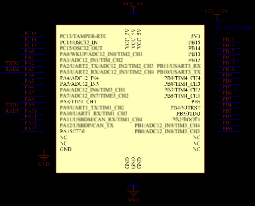
The interface circuit diagram of the STM32F103C8T6 microcontroller core board is shown below.
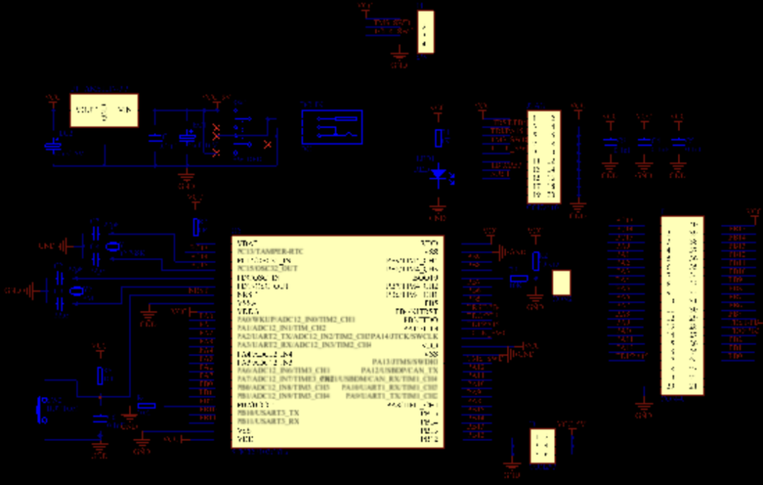
The internal circuit diagram of the STM32 microcontroller core board is shown below.
Button circuit (including pull-up resistor) design
The touch button is a classified product under button products, which acts as an electronic switch. Just pressing the button lightly can connect the switch, and it disconnects when released. The principle is mainly achieved by the internal metal spring of the touch button being pressed to realize the connection and disconnection.
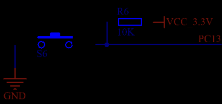
The button serves as the input for the system, acting as a hub for human-computer interaction. The microcontroller control pin for the button defaults to a high level, and when the button is pressed, the relevant pin of the microcontroller changes to a low level.
This enables manual input to the system. Its circuit schematic is shown below. The resistor in the circuit serves as a pull-up resistor to ensure stable output of the button signal.
MFRC-522 RFID Module Circuit Design
The MFRC-522 radio frequency module is chosen for card swiping operations. The MFRC522 is a highly integrated read/write card chip for 13.56MHz non-contact communication, designed by NXP for low voltage, low cost, and compact size applications, making it a good choice for smart instruments and portable handheld devices.
The MFRC522 utilizes advanced modulation and demodulation concepts, fully integrating all types of passive non-contact communication methods and protocols at 13.56MHz. It supports ISO14443A compatible responder signals. The digital part processes ISO14443A frames and error detection.
Additionally, it supports the fast CRYPTO1 encryption algorithm for verifying MIFARE series products.
The MFRC522 supports higher-speed non-contact communication for MIFARE series, with a bidirectional data transfer rate of up to 424kbit/s. As a new member of the 13.56MHz high-integrated read/write card series chip family, the MFRC522 shares many similarities with the MFRC500 and MFRC530, while also possessing many unique features and differences.
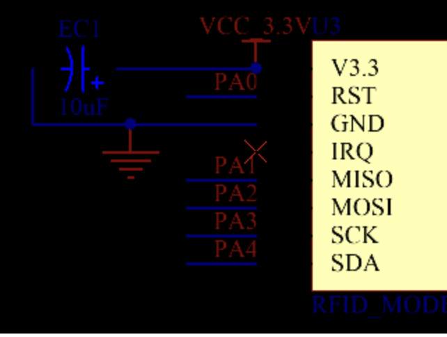
It communicates with the host using SPI mode, which helps reduce wiring, shrink PCB size, and lower costs.
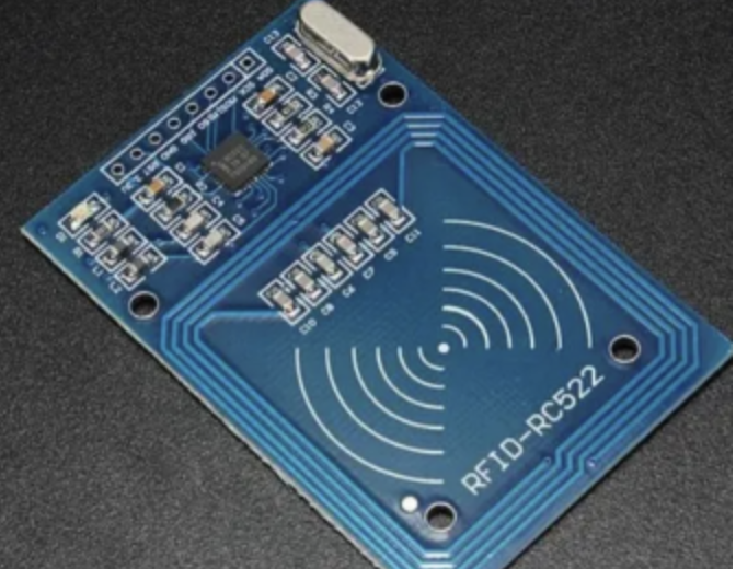
The MF522-AN module uses the original Philips MFRC522 chip to design the card reading circuit, is easy to use, low-cost, and suitable for users needing to develop devices, card readers, or design/produce RFID card terminals.
This module can be directly inserted into various card reader molds. The module operates at 3.3V and can be connected to any CPU motherboard with just a few simple lines through the SPI interface, ensuring the module works stably and reliably with a long reading distance;
Electrical Parameter Overview
(1) Operating current: 13—26mA/DC 3.3V
(2) Idle current: 10-13mA/DC 3.3V
(3) Sleep current: <80uA
(4) Peak current: <30mA
(5) Operating frequency: 13.56MHz
(6) Supported card types: mifare1 S50, mifare1 S70, mifare UltraLight, mifare Pro, mifare Desfire
(7) Operating temperature: -20—80 degrees Celsius
(8) Storage temperature: -40—85 degrees Celsius
(9) Relative humidity:
(10) Relative humidity 5%—95%
Module Interface SPI Parameters
Data transfer rate: up to 10Mbit/s
Main Indicators of the Module
Capacity of 8K bits EEPROM
Divided into 16 sectors, each sector consists of 4 blocks, each block 16 bytes, accessed by blocks
Each sector has its own set of passwords and access control
Each card has a unique serial number, 32 bits
Supports anti-collision mechanism, allows multiple card operations
No power supply, self-contained antenna, includes encryption control logic and communication logic circuit
Data retention period of 10 years, rewritable 100,000 times, read unlimited times
Operating temperature: -20℃~50℃ (humidity 90%)
Operating frequency: 13.56MHZ
Communication rate: 106 KBPS
Reading distance: within 10 cm (related to the reader)
Module Interface Schematic
Physical Image of the Module
5V Relay Control Circuit
A relay is an electric control device that causes a predetermined step change in the electrical output circuit when the input quantity (excitation quantity) changes to meet specified requirements.
It has an interactive relationship between the control system (also known as the input circuit) and the controlled system (also known as the output circuit).
It is commonly used in automated control circuits and acts as an “automatic switch” that uses a small current to control a large current operation. The relay is an automatic switch element with isolation functions, widely used in remote control, telemetry, communications, automation, mechatronics, and power electronic devices, making it one of the most important control components, playing roles in automatic regulation, safety protection, and circuit switching.
Relays generally consist of an iron core, coil, armature, contact springs, etc. As long as a certain voltage is applied across the coil, a certain current will flow through the coil, generating electromagnetic effects. The armature will be attracted by the electromagnetic force to overcome the return spring’s pull, bringing the armature’s moving contact to engage with the static contact (normally open contact).
When the coil is powered off, the electromagnetic force disappears, and the armature returns to its original position under the spring’s reaction force, releasing the moving contact from the original static contact (normally closed contact). This engaging and releasing achieves the purpose of connecting and disconnecting in the circuit.
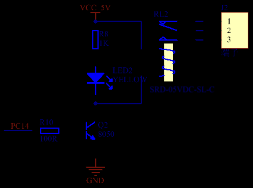
In this system, the relay is driven by a transistor. When the control pin of the microcontroller is at a high level, the transistor conducts, powering the relay to close while the indicator LED lights up. The resistor in series with the LED serves to limit current and protect the LED, while the resistor connected to the base of the transistor also serves to limit current and protect the transistor. The principle diagram of the relay control circuit is shown below.
Software Design
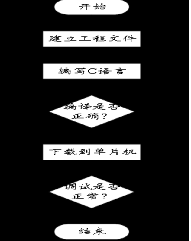
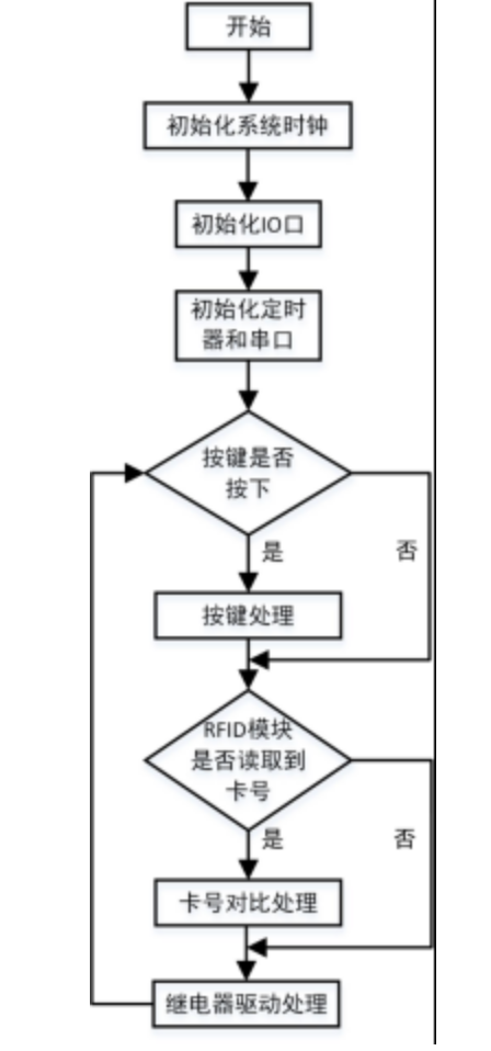
Program Flowchart
Code
main.c
#include "led.h"
#include "delay.h"
#include "sys.h"
#include "usart.h"
#include "lcd.h"
#include <stdio.h>
#include "timer.h"
#include "lcd1602.h"
#include "key.h"
#include "rc522.h"
/**************/unsigned char idCard[4]={0x87,0x15,0xc9,0x73};        //Valid card number/**************/
u8 rekey = 0;//Prevent key repeat
tu8 i;
unsigned char UID[5];            //Read card number
unsigned char Temp[4];
int main(void){          delay_init();             //Initialize delay function          uart_init(9600);         //Initialize serial port to 9600  TIM3_Int_Init(499,7199);//50ms           LED_Init();                  //Initialize hardware interface connected to LED    KEY_Init();            //Initialize button
    relay1 = 0;      delay_ms(200);    relay1 =1;
  Rc522IoInit();  PcdReset();//Reset RC522  PcdAntennaOn();//Turn on antenna emission
     while(1)    {        if(key1==0)         //Detect button press        {            delay_ms(10);   //Small debounce
                if(key1==0)    //Check if pressed                {                    relay1 =1;    //Open relay            }        }    if(PcdRequest(0x52,Temp)==MI_OK)//Read card    {      if(PcdAnticoll(UID)==MI_OK)//Card number acquisition successful      {                 if((UID[0]==idCard[0])&&(UID[2]==idCard[2])&&(UID[3]==idCard[3]))//Match card number                {                    relay1 =0;        //Close relay                }                        delay_ms(10);      }    }
    }                                                }
lcd1602.h
#include "lcd1602.h"
/************************Port Initialization*******************************/void Lcd_GPIO_init(void){     GPIO_InitTypeDef GPIO_InitStructure;   //Declare structure
    /********Data port settings*************/     RCC_APB2PeriphClockCmd(RCC_GPIO_DATA, ENABLE);  //Enable port B clock      GPIO_InitStructure.GPIO_Pin  = GPIO_DATA_0_PIN|GPIO_DATA_1_PIN|GPIO_DATA_2_PIN|GPIO_DATA_3_PIN|GPIO_DATA_4_PIN|GPIO_DATA_5_PIN|GPIO_DATA_6_PIN|GPIO_DATA_7_PIN; //  DB8~DB15     GPIO_InitStructure.GPIO_Mode = GPIO_Mode_Out_PP;  //Standard output mode     GPIO_InitStructure.GPIO_Speed = GPIO_Speed_50MHz; //50M clock speed     GPIO_Init(GPIO_DATA_0, &GPIO_InitStructure);      //Initialize port
     /********Enable port settings**********/     RCC_APB2PeriphClockCmd(RCC_GPIO_EN, ENABLE);        //Enable port clock      GPIO_InitStructure.GPIO_Pin =  GPIO_EN_PIN;         //  Enable port     GPIO_InitStructure.GPIO_Mode = GPIO_Mode_Out_PP;  //Standard output mode     GPIO_InitStructure.GPIO_Speed = GPIO_Speed_50MHz; //50M clock speed     GPIO_Init(GPIO_EN, &GPIO_InitStructure);
     /********Read/Write port settings**********/     RCC_APB2PeriphClockCmd(RCC_GPIO_RW, ENABLE);    //Enable port clock      GPIO_InitStructure.GPIO_Pin =  GPIO_RW_PIN;     //  Enable port     GPIO_InitStructure.GPIO_Mode = GPIO_Mode_Out_PP;  //Standard output mode     GPIO_InitStructure.GPIO_Speed = GPIO_Speed_50MHz; //50M clock speed     GPIO_Init(GPIO_RW, &GPIO_InitStructure);
     /********Instruction/Data port settings**********/     RCC_APB2PeriphClockCmd(RCC_GPIO_RS, ENABLE);    //Enable port clock      GPIO_InitStructure.GPIO_Pin =  GPIO_RS_PIN;     //  Enable port     GPIO_InitStructure.GPIO_Mode = GPIO_Mode_Out_PP; //Push-pull multiplex output     GPIO_InitStructure.GPIO_Speed = GPIO_Speed_50MHz; //50M clock speed     GPIO_Init(GPIO_RS, &GPIO_InitStructure);
}/******************************************************************/

void Lcd_Init( void )  //Initialization{       Lcd_GPIO_init();    delay_us(1500);                     //Delay 15ms    Lcd_Write_Command( 0x38,0);       // Write command 38H without checking busy signal    delay_us(500);                      //Delay 5ms    Lcd_Write_Command( 0x38,0);       // Write command 38H without checking busy signal    delay_us(500);                      //Delay 5ms    Lcd_Write_Command( 0x38,0);       // Write command 38H without checking busy signal                                         //Each time before writing a command or reading/writing data, the busy signal must be checked    Lcd_Write_Command( 0x38,1);       //Display mode settings     Lcd_Write_Command( 0x08,1);          //Display off    Lcd_Write_Command( 0x01,1);       //Clear display    Lcd_Write_Command( 0x06,1);       //Cursor movement settings     Lcd_Write_Command( 0x0C,1);       //Display on, cursor not displayed}
/******************************************************/
void Lcd_En_Toggle(void) //Send enable pulse{    SET_EN;        //Enable 1    delay_us(5);   //Delay 160us    CLE_EN;}

void Lcd_Busy(void)//Check busy{     unsigned int later0=0;     GPIO_InitTypeDef GPIO_InitStructure;     RCC_APB2PeriphClockCmd(RCC_GPIO_DATA, ENABLE);    //Enable DATA port clock
     GPIO_InitStructure.GPIO_Pin  = GPIO_DATA_0_PIN|GPIO_DATA_1_PIN|GPIO_DATA_2_PIN|GPIO_DATA_3_PIN|GPIO_DATA_4_PIN|GPIO_DATA_5_PIN|GPIO_DATA_6_PIN|GPIO_DATA_7_PIN; //  DB8~DB15     GPIO_InitStructure.GPIO_Mode = GPIO_Mode_IPU; //Input mode = Pull-up input     GPIO_InitStructure.GPIO_Speed = GPIO_Speed_50MHz; //50M clock speed     GPIO_Init(GPIO_DATA_7, &GPIO_InitStructure);      //Open busy detection port
      CLE_RS; //RS = 0     //delay_us(1);   //Delay 10us     SET_RW; //RW = 1     //delay_us(1);   //Delay 10us     SET_EN; //EN = 1     //delay_us(2);   //Delay 20us     while ((GPIO_ReadInputDataBit(GPIO_DATA_7,GPIO_DATA_7_PIN))&&(later0<20000)) //Loop waiting for busy detection port = 0     {         delay_us(5);        later0++;         }     CLE_EN; //EN = 0
     //Restore port to output state         RCC_APB2PeriphClockCmd(RCC_GPIO_DATA, ENABLE);    //Enable DATA port clock      GPIO_InitStructure.GPIO_Pin  = GPIO_DATA_0_PIN|GPIO_DATA_1_PIN|GPIO_DATA_2_PIN|GPIO_DATA_3_PIN|GPIO_DATA_4_PIN|GPIO_DATA_5_PIN|GPIO_DATA_6_PIN|GPIO_DATA_7_PIN; //  DB8~DB15     GPIO_InitStructure.GPIO_Mode = GPIO_Mode_Out_PP; //Push-pull output     GPIO_InitStructure.GPIO_Speed = GPIO_Speed_50MHz; //50M clock speed     GPIO_Init(GPIO_DATA_7, &GPIO_InitStructure);
}
void Gpio_data(unsigned char x)  //Set data to port{  GPIO_ResetBits(GPIO_DATA_0, GPIO_DATA_0_PIN);  //DB0GPIO_ResetBits(GPIO_DATA_0, GPIO_DATA_1_PIN);  //DB1GPIO_ResetBits(GPIO_DATA_0, GPIO_DATA_2_PIN);  //DB2GPIO_ResetBits(GPIO_DATA_0, GPIO_DATA_3_PIN);  //DB3GPIO_ResetBits(GPIO_DATA_0, GPIO_DATA_4_PIN);  //DB4GPIO_ResetBits(GPIO_DATA_0, GPIO_DATA_5_PIN);  //DB5GPIO_ResetBits(GPIO_DATA_0, GPIO_DATA_6_PIN);  //DB6GPIO_ResetBits(GPIO_DATA_0, GPIO_DATA_7_PIN);  //DB7if(x&&0X01)GPIO_SetBits(GPIO_DATA_0, GPIO_DATA_0_PIN);//DB0if(x&&0X02)GPIO_SetBits(GPIO_DATA_0, GPIO_DATA_1_PIN);//DB1if(x&&0X04)GPIO_SetBits(GPIO_DATA_0, GPIO_DATA_2_PIN);//DB2if(x&&0X08)GPIO_SetBits(GPIO_DATA_0, GPIO_DATA_3_PIN);//DB3if(x&&0X10)GPIO_SetBits(GPIO_DATA_0, GPIO_DATA_4_PIN);//DB4if(x&&0X20)GPIO_SetBits(GPIO_DATA_0, GPIO_DATA_5_PIN);//DB5if(x&&0X40)GPIO_SetBits(GPIO_DATA_0, GPIO_DATA_6_PIN);//DB6if(x&&0X80)GPIO_SetBits(GPIO_DATA_0, GPIO_DATA_7_PIN);//DB7}

//Write command to LCD, timing: RS=L, RW=L, Data0-Data7=command code, E=high pulsevoid Lcd_Write_Command(unsigned char x,char Busy) {     if(Busy) Lcd_Busy();    //delay_us(1);   //Delay 10us    CLE_RS;  //RS = 0     //delay_us(1);   //Delay 10us    CLE_RW;  //RW = 0     //delay_us(4);   //Delay 40us    Gpio_data(x);  //Set data to port    //delay_us(4);   //Delay 40us    Lcd_En_Toggle();  //Send enable pulse    //delay_us(1);   //Delay 100us    Lcd_Busy(); //Check busy
}//Write data to LCD, timing: RS=H, RW=L, Data0-Data7=data code, E=high pulsevoid Lcd_Write_Data( unsigned char x) //Write data to LCD {     Lcd_Busy(); //Check busy    //delay_us(1);   //Delay 10us    SET_RS;   //RS = 1     //delay_us(1);   //Delay 10us    CLE_RW;   //RW = 0    //delay_us(4);   //Delay 40us    Gpio_data(x);    //delay_us(4);   //Delay 40us    Lcd_En_Toggle();  //Send enable pulse    //delay_us(1);   //Delay 100us    Lcd_Busy(); //Check busy
}
void Lcd_SetXY(unsigned char x,unsigned char y)   //Set initial position of character, x represents column, y represents row {      unsigned char addr;      if(y==0)           addr=0x80+x;      else if(y==1)          addr=0xC0+x;      Lcd_Write_Command(addr,1) ; }
/******************************************************/
void Lcd_Puts(unsigned char x,unsigned char y, unsigned char *string) //Write a string to 1602 {    //unsigned char i=0;   Lcd_SetXY(x,y);     while(*string)       {        Lcd_Write_Data(*string);        string++;       } }
void Lcd_1Put(unsigned char x,unsigned char y, unsigned char Data0){       Lcd_SetXY(x,y);     Lcd_Write_Data(Data0); }
lcd1602.h
#ifndef __lcd1602_H
#define __lcd1602_H
#include "stm32f10x.h"
#include "delay.h"
/********************Port Definitions*********************************/#define GPIO_EN       GPIOB                 //  Enable port group#define GPIO_EN_PIN   GPIO_Pin_7            //  Enable port number#define RCC_GPIO_EN   RCC_APB2Periph_GPIOB  //  Enable clock group
#define GPIO_RW       GPIOB                 //  Read/Write select port group#define GPIO_RW_PIN   GPIO_Pin_6            //  Read/Write select port number#define RCC_GPIO_RW   RCC_APB2Periph_GPIOB  //  Read/Write clock group
#define GPIO_RS       GPIOB                 //  Data/Command port group#define GPIO_RS_PIN   GPIO_Pin_5            //  Data/Command port number#define RCC_GPIO_RS   RCC_APB2Periph_GPIOB  //  Data/Command clock group
#define GPIO_DATA_0       GPIOB         //  Data line 0_port group#define GPIO_DATA_0_PIN   GPIO_Pin_8    //  Data line 0_port number#define GPIO_DATA_1       GPIOB         //  Data line 1_port group0#define GPIO_DATA_1_PIN   GPIO_Pin_9    //  Data line 1_port number#define GPIO_DATA_2       GPIOB         //  Data line 2_port group#define GPIO_DATA_2_PIN   GPIO_Pin_10   //  Data line 2_port number#define GPIO_DATA_3       GPIOB         //  Data line 3_port group#define GPIO_DATA_3_PIN   GPIO_Pin_11   //  Data line 3_port number#define GPIO_DATA_4       GPIOB         //  Data line 4_port group#define GPIO_DATA_4_PIN   GPIO_Pin_12   //  Data line 4_port number#define GPIO_DATA_5       GPIOB         //  Data line 5_port group#define GPIO_DATA_5_PIN   GPIO_Pin_13   //  Data line 5_port number#define GPIO_DATA_6       GPIOB         //  Data line 6_port group#define GPIO_DATA_6_PIN   GPIO_Pin_14   //  Data line 6_port number#define GPIO_DATA_7       GPIOB         //  Data line 7_port group#define GPIO_DATA_7_PIN   GPIO_Pin_15   //  Data line 7_port number#define RCC_GPIO_DATA   RCC_APB2Periph_GPIOB  //  Data line clock group
/******************************************************************/

/***********************Basic Commands***********************************/#define SET_EN  GPIO_SetBits(GPIO_EN, GPIO_EN_PIN)        //EN Enable  Output1#define CLE_EN  GPIO_ResetBits(GPIO_EN, GPIO_EN_PIN)    //      Output0 #define SET_RW  GPIO_SetBits(GPIO_RW, GPIO_RW_PIN)      //RW Read/Write  Output1#define CLE_RW  GPIO_ResetBits(GPIO_RW, GPIO_RW_PIN)    //      Output0#define SET_RS  GPIO_SetBits(GPIO_RS, GPIO_RS_PIN)        //RS Command  Output1#define CLE_RS  GPIO_ResetBits(GPIO_RS, GPIO_RS_PIN)    //      Output0/******************************************************************/
void Lcd_GPIO_init(void);
void Lcd_Init( void ) ;
void Lcd_En_Toggle(void);
void Lcd_Busy(void);
void Gpio_data(unsigned char x);
void Lcd_Write_Command(unsigned char x,char Busy);
void Lcd_Write_Data( unsigned char x);
void Lcd_SetXY(unsigned char x,unsigned char y);
void Lcd_Puts(unsigned char x,unsigned char y, unsigned char *string);
void Lcd_1Put(unsigned char x,unsigned char y, unsigned char Data0);

#endif
rc552.c
#include "rc522.h"
void Rc522IoInit(void){// P4DIR |= BIT7+BIT6+BIT5+BIT3; //Card reading interface// P4DIR &=~BIT4;
GPIO_InitTypeDef GPIO_InitStructure;
RCC_APB2PeriphClockCmd(RCC_APB2Periph_GPIOA, ENABLE); //Enable PA, PD port clock
GPIO_InitStructure.GPIO_Pin = GPIO_Pin_0|GPIO_Pin_2|GPIO_Pin_3|GPIO_Pin_4; // Port configuration GPIO_InitStructure.GPIO_Mode = GPIO_Mode_Out_PP; //Push-pull output GPIO_InitStructure.GPIO_Speed = GPIO_Speed_50MHz; //IO speed is 50MHz GPIO_Init(GPIOA, &GPIO_InitStructure); //Initialize according to set parameters
RCC_APB2PeriphClockCmd(RCC_APB2Periph_GPIOA,ENABLE);//Enable PORTA,PORTC clock
GPIO_InitStructure.GPIO_Pin = GPIO_Pin_1;//PA1 GPIO_InitStructure.GPIO_Mode = GPIO_Mode_IPU; //Set to pull-up input GPIO_Init(GPIOA, &GPIO_InitStructure);//Initialize GPIOA15
}
//******************************************************************///Function: Read RC522 register//Parameter description: Address[IN]: Register address//Return: Read value//******************************************************************/
unsigned char ReadRawRC(unsigned char Address){ unsigned char i, ucAddr ; unsigned char ucResult=0 ; NSS522_0 ; SCK522_0 ; ucAddr = ((Address<<1)&&0x7E)|0x80 ; for(i=8;i>0;i--) { if((ucAddr&&0x80)==0x80) SI522_1 ; else SI522_0 ; SCK522_1 ; ucAddr <<= 1 ; SCK522_0 ; } for(i=8;i>0;i--) { SCK522_1 ; ucResult <<=1 ; ucResult |= SO522 ; SCK522_0 ; } SCK522_0 ; NSS522_1 ; return ucResult ;}
//******************************************************************///Function: Write to RC522 register//Parameter description: Address[IN]: Register address// value Value to write//******************************************************************/
void WriteRawRC(unsigned char Address, unsigned char value){ unsigned char ucAddr ;
NSS522_0 ; SCK522_0 ; ucAddr = ((Address<<1)&&0x7E) ; { if(ucAddr&&0x80) SI522_1 ; else SI522_0 ; SCK522_1 ; ucAddr <<= 1 ; SCK522_0 ;
if(ucAddr&&0x80) SI522_1 ; else SI522_0 ; SCK522_1 ; ucAddr <<= 1 ; SCK522_0 ;
if(ucAddr&&0x80) SI522_1 ; else SI522_0 ; SCK522_1 ; ucAddr <<= 1 ; SCK522_0 ;
if(ucAddr&&0x80) SI522_1 ; else SI522_0 ; SCK522_1 ; ucAddr <<= 1 ; SCK522_0 ;
if(ucAddr&&0x80) SI522_1 ; else SI522_0 ; SCK522_1 ; ucAddr <<= 1 ; SCK522_0 ;
if(ucAddr&&0x80) SI522_1 ; else SI522_0 ; SCK522_1 ; ucAddr <<= 1 ; SCK522_0 ;
if(ucAddr&&0x80) SI522_1 ; else SI522_0 ; SCK522_1 ; ucAddr <<= 1 ; SCK522_0 ;
if(ucAddr&&0x80) SI522_1 ; else SI522_0 ; SCK522_1 ; ucAddr <<= 1 ; SCK522_0 ; } { if(value&&0x80) SI522_1 ; else SI522_0 ; SCK522_1 ; value <<= 1 ; SCK522_0 ;
if(value&&0x80) SI522_1 ; else SI522_0 ; SCK522_1 ; value <<= 1 ; SCK522_0 ;
if(value&&0x80) SI522_1 ; else SI522_0 ; SCK522_1 ; value <<= 1 ; SCK522_0 ;
if(value&&0x80) SI522_1 ; else SI522_0 ; SCK522_1 ; value <<= 1 ; SCK522_0 ;
if(value&&0x80) SI522_1 ; else SI522_0 ; SCK522_1 ; value <<= 1 ; SCK522_0 ;
if(value&&0x80) SI522_1 ; else SI522_0 ; SCK522_1 ; value <<= 1 ; SCK522_0 ;
if(value&&0x80) SI522_1 ; else SI522_0 ; SCK522_1 ; value <<= 1 ; SCK522_0 ;
if(value&&0x80) SI522_1 ; else SI522_0 ; SCK522_1 ; value <<= 1 ; SCK522_0 ; } SCK522_0; NSS522_1;}
//******************************************************************///Function: Set RC522 register bit//Parameter description: reg[IN]: Register address// mask[IN]: Set bit value//******************************************************************/
void SetBitMask(unsigned char reg,unsigned char mask) { char tmp = 0x0 ; tmp = ReadRawRC(reg)| mask; WriteRawRC(reg,tmp | mask); // set bit mask}
//******************************************************************///Function: Clear RC522 register bit//Parameter description: reg[IN]: Register address// mask[IN]: Clear bit value//******************************************************************/
void ClearBitMask(unsigned char reg,unsigned char mask) { char tmp = 0x0 ; tmp = ReadRawRC(reg)&&(~mask); WriteRawRC(reg, tmp) ; // clear bit mask}
//******************************************************************///Function: Reset RC522//Return: Successfully returns MI_OK//******************************************************************/#define DELAYNUM 200char PcdReset(){ RF_POWER_ON ; RST522_1 ; delay_us(DELAYNUM) ; RST522_0 ; delay_us(DELAYNUM) ; RST522_1 ; delay_us(DELAYNUM) ; WriteRawRC(CommandReg,PCD_RESETPHASE); delay_us(DELAYNUM) ; WriteRawRC(ModeReg,0x3D) ; WriteRawRC(TReloadRegL,30) ; WriteRawRC(TReloadRegH,0) ; WriteRawRC(TModeReg,0x8D) ; WriteRawRC(TPrescalerReg,0x3E) ; // WriteRawRC(TxASKReg,0x40) ; // FOR DEBUG AND TEST return MI_OK ; }
//******************************************************************///Turn on antenna emission //There should be at least a 1ms interval between starting or stopping antenna emission//******************************************************************/void PcdAntennaOn(){ unsigned char i; WriteRawRC(TxASKReg,0x40) ; delay_us(800);//delay_ms(1) ; i = ReadRawRC(TxControlReg) ; if(!(i&&0x03)) SetBitMask(TxControlReg, 0x03); i=ReadRawRC(TxASKReg) ;}
//******************************************************************///Turn off antenna emission//******************************************************************///void PcdAntennaOff()//{// ClearBitMask(TxControlReg, 0x03);//}
//******************************************************************///Function: Communicate through RC522 and ISO14443 card//Parameter description: Command[IN]: RC522 command word// pInData[IN]: Data sent to the card through RC522// InLenByte[IN]: Length of data to be sent in bytes// pOutData[OUT]: Data returned from the card// *pOutLenBit[OUT]: Length of returned data in bits//******************************************************************/char PcdComMF522(unsigned char Command ,unsigned char *pInData , unsigned char InLenByte,unsigned char *pOutData, unsigned int *pOutLenBit ){ char status = MI_ERR ; unsigned char irqEn = 0x00 ; unsigned char waitFor = 0x00 ; unsigned char lastBits ; unsigned char n ; unsigned int i ; switch (Command) { case PCD_AUTHENT: irqEn = 0x12 ; waitFor = 0x10 ; break ; case PCD_TRANSCEIVE: irqEn = 0x77 ; waitFor = 0x30 ; break ; default: break ; } WriteRawRC(ComIEnReg,irqEn|0x80) ; // ClearBitMask(ComIrqReg,0x80) ; WriteRawRC(CommandReg,PCD_IDLE) ; SetBitMask(FIFOLevelReg,0x80) ; // Clear FIFO for(i=0; i<InLenByte; i++) WriteRawRC(FIFODataReg,pInData[i]) ; // Write data to FIFO WriteRawRC(CommandReg, Command) ; // Write command to command register if(Command == PCD_TRANSCEIVE) SetBitMask(BitFramingReg,0x80) ; // Start sending i = 6000 ; //Adjust according to clock frequency, maximum wait time for M1 card is 25ms do { n = ReadRawRC(ComIrqReg) ; i-- ; } while((i!=0)&&!(n&&0x01)&&!(n&&waitFor)) ; ClearBitMask(BitFramingReg,0x80) ; if(i!=0) { if(!(ReadRawRC(ErrorReg)&&0x1B)) { status = MI_OK ; if (n&&irqEn&&0x01) status = MI_NOTAGERR ; if(Command==PCD_TRANSCEIVE) { n = ReadRawRC(FIFOLevelReg) ; lastBits = ReadRawRC(ControlReg)&&0x07 ; if(lastBits) *pOutLenBit = (n-1)*8 + lastBits ; else *pOutLenBit = n*8 ; if(n==0) n = 1 ; if(n>MAXRLEN) n = MAXRLEN ; for (i=0; i<n; i++) pOutData[i] = ReadRawRC(FIFODataReg) ; } } else status = MI_ERR ; } SetBitMask(ControlReg,0x80) ;// stop timer now WriteRawRC(CommandReg,PCD_IDLE) ; return status;}
//******************************************************************///Function: Search card ///Parameter description: req_code[IN]: Card searching method /// 0x52 = Search all cards that comply with ISO14443A standard in the induction area /// 0x26 = Search cards that have not entered sleep mode /// pTagType[OUT]: Card type code /// 0x4400 = Mifare_UltraLight /// 0x0400 = Mifare_One(S50) /// 0x0200 = Mifare_One(S70) /// 0x0800 = Mifare_Pro(X) /// 0x4403 = Mifare_DESFire ///Return: Successfully returns MI_OK ///******************************************************************/char PcdRequest(unsigned char req_code,unsigned char *pTagType){ char status ; unsigned int unLen ; unsigned char ucComMF522Buf[MAXRLEN] ;
PcdReset();//Reset RC522 PcdAntennaOn();//Turn on antenna emission delay_ms(1);
ClearBitMask(Status2Reg,0x08) ; WriteRawRC(BitFramingReg,0x07) ; SetBitMask(TxControlReg,0x03) ;
ucComMF522Buf[0] = req_code ;
status = PcdComMF522(PCD_TRANSCEIVE,ucComMF522Buf, 1,ucComMF522Buf,&unLen ); if ((status == MI_OK) && (unLen == 0x10)) { *pTagType = ucComMF522Buf[0] ; *(pTagType+1) = ucComMF522Buf[1] ; } else status = MI_ERR ; return status ;}
//******************************************************************///Function: Anti-collision ///Parameter description: pSnr[OUT]: Card serial number, 4 bytes ///Return: Successfully returns MI_OK ///******************************************************************/char PcdAnticoll(unsigned char *pSnr){ char status; unsigned char i,snr_check=0; unsigned int unLen; unsigned char ucComMF522Buf[MAXRLEN];
ClearBitMask(Status2Reg,0x08); WriteRawRC(BitFramingReg,0x00); ClearBitMask(CollReg,0x80);
ucComMF522Buf[0] = PICC_ANTICOLL1; ucComMF522Buf[1] = 0x20;
status = PcdComMF522(PCD_TRANSCEIVE,ucComMF522Buf,2,ucComMF522Buf,&unLen);
if (status == MI_OK) { for (i=0; i<4; i++) { *(pSnr+i) = ucComMF522Buf[i]; snr_check ^= ucComMF522Buf[i]; } if (snr_check != ucComMF522Buf[i]) { status = MI_ERR; } }
SetBitMask(CollReg,0x80); return status;}

↑ Hot Course, Limited Time Coupon! 🎉 Grab it Quickly ↑