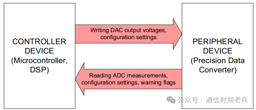
In this article, we will introduce the basics of digital communication and the Serial Peripheral Interface (SPI) communication. This includes the communication structure and the required digital lines.Many precision analog devices have digital interfaces between microcontrollers (referred to as controllers) and controlled devices (referred to as peripherals). For example, a precision Analog-to-Digital Converter (ADC) measures the input voltage, while the controller microcontroller reads this data through digital communication. As a second example, the controller microcontroller writes a digital word to a Digital-to-Analog Converter (DAC) to set the output voltage. In both types of devices, this communication can be bidirectional.
Many precision data converters may require some configuration and programming. Writing and reading operations need to be performed on the device, thus requiring digital communication. To enable communication between two devices, a common standard is needed so that the controller and peripheral can understand each other.
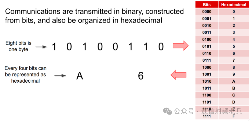
Communication is transmitted through words represented in binary. These communication bits consist of 1s and 0s, typically organized into groups of 8 bits, known as a byte. For convenience, bytes can be organized into two hexadecimal numbers. Usually, when sending and receiving data between the microcontroller (controller) and peripherals, multiple bytes are used. Multiple bytes may be used to represent the output data of the ADC, the output voltage of the DAC, or to send commands and configuration information to the data converters.
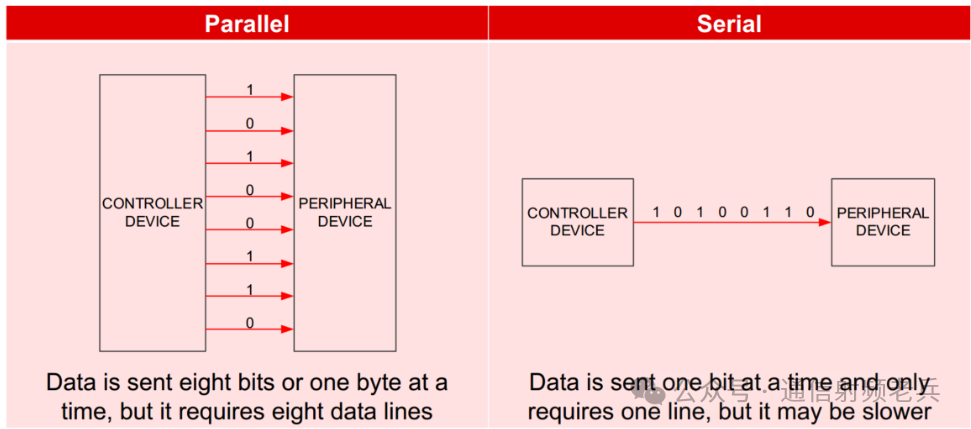
Digital communication can take various forms, but primarily two structures are commonly used. First, communication can be parallel, where each bit of data uses a separate line. For example, a byte is transmitted simultaneously through eight parallel digital lines. Secondly, communication can be serial, where all data bits are sent over the same digital line. In serial communication, the data bits are sent one after another in sequence.
In modern devices, serial communication is more widely used, reducing the number of communication lines between the controller and peripherals. The illustration here shows the process of data being transmitted from the controller to the peripheral, but transmitting data back from the peripheral to the controller requires separate lines. Most precision data converters use serial communication.
Most device manufacturers use one of two different serial interface standards, either the 4-wire Serial Peripheral Interface (SPI) or the 2-wire I2C.
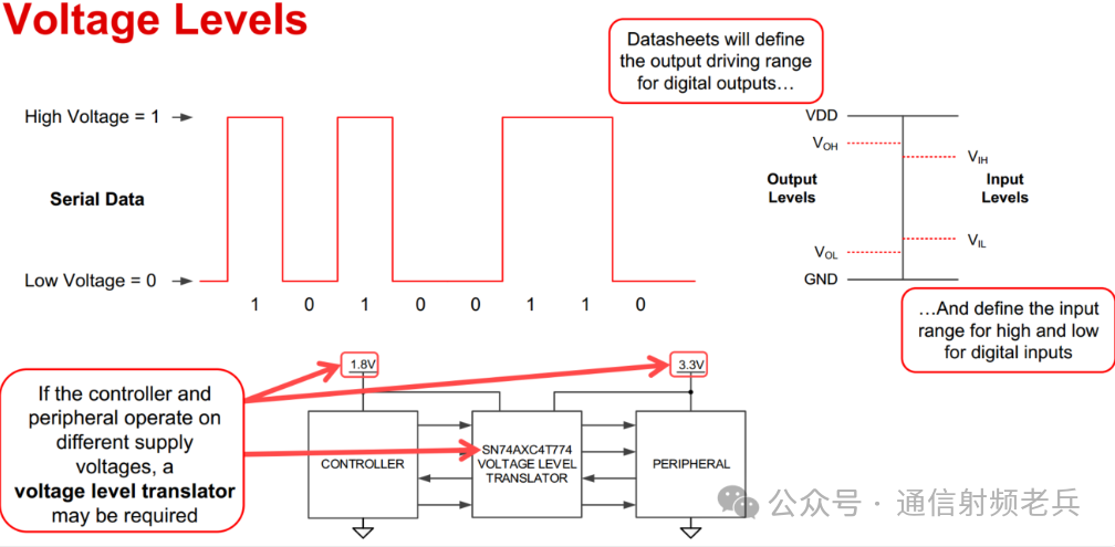
The lines between the controller and the peripheral are driven to one of two voltage levels. If the voltage is close to 0, the line is decoded as a digital 0. If the voltage is close to the digital supply voltage, the line is decoded as a digital 1. Note that both the controller and the peripheral need to agree on these levels to ensure that communication can be correctly decoded. Digital outputs must be driven to a sufficiently high level to be decoded as a digital 1 and driven to a sufficiently low level to be decoded as a digital 0.
The data sheet defines the minimum high-level output voltage and maximum low-level output voltage for digital outputs. Additionally, the data sheet defines the minimum input voltage for defining high levels and the maximum input voltage for defining low levels. Their communication standards define these levels based on the digital supply voltage. If the digital supply voltages of the controller and peripheral do not match, communication issues may arise. In this case, a level-shifting device may be needed to bridge communication from one supply voltage to another.
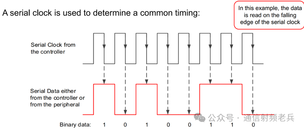
Communication also requires a common timing between the controller and the peripheral. Both devices must agree on timing, meaning they need to know when the peripheral should read the voltage levels to determine when bit transmission occurs. Typically, a serial clock from the controller is used to define the timing of the communication. Bits may be read on the rising or falling edge of the serial clock. In this example, data is read on the falling edge of the serial clock.
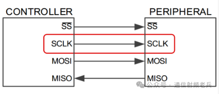
The most commonly used serial interface in precision data converters is a standard known as the Serial Peripheral Interface (SPI). SPI has two control lines. The controller (usually a microcontroller or digital signal processor) controls the slave select and the serial clock used for data synchronization. One SPI bus can control multiple peripherals, but there can only be one controller. Each peripheral needs to receive its own slave select line from the controller.
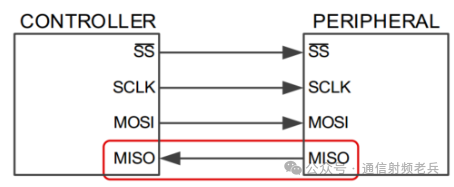
Additionally, there are two data lines. One line is used to send data from the controller to the peripheral, while the other line is used to send data from the peripheral to the controller. Data transmission can be full-duplex, meaning data can be transmitted in both directions using the same SCLK pulse. The four lines of SPI will be described next.
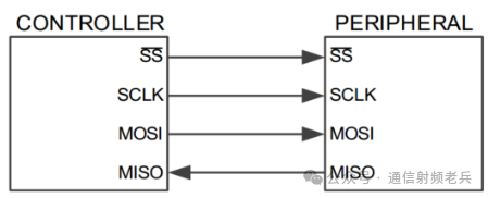
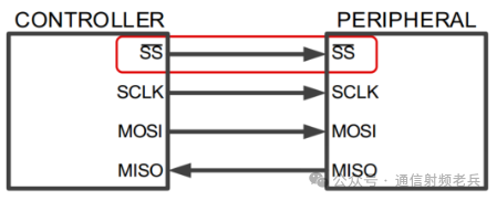
SS (Slave Select) is the peripheral select line. This line is used to select the peripheral to communicate with. If there are multiple devices on the SPI bus, each device has its own peripheral select line. The peripheral select line is typically active low, indicated by an overline.
When a device is selected, the peripheral select line goes low to activate communication. When the device is not selected, the peripheral select line is set high. The peripheral select line may also be labeled as SSEL, CS, CS# (CS bar, indicating active low), CE, nSS, or SS#. In many precision ADCs from Texas Instruments (TI), this chip select line is often labeled as CS# (CS bar) and is active low. In many precision DACs, this line is often labeled as SYNC# (SYNC bar), also active low.
SCLK is the serial clock. As mentioned earlier, SCLK is used by the controller to synchronize the data being sent between the controller and the peripheral. SCLK originates from the controller and is sent to all peripherals. This serial clock is not always active; it may be idle as either a high or low signal. Data is fed into the controller or peripheral on the rising or falling edge of the serial clock. The SCLK line may also be labeled as SCK.
MISO (Master In Slave Out) is the controller input, peripheral output line. This line is used to send data from the peripheral device to the controller. If the controller has not selected the device as active via the peripheral select line, this line goes to a high-impedance state (Hi-Z), allowing systems with multiple devices to share this line.
The peripheral device sends data on the MISO line, synchronized with SCLK. On the peripheral device, it may be referred to as SOMI, SDO, DO, DOUT, or SO. This line connects to a serial interface on the controller device labeled SDI, DI, or DN. In many precision data converters, this digital output is typically labeled as DOUT.
The data between the controller and peripheral can be read on the rising or falling edge of SCLK. Additionally, the clock polarity is very important in defining the leading and trailing edges of data entering and exiting the device. This allows SPI communication to have multiple modes.
There are two parameters used to determine the operating mode. The first parameter is CPOL, which determines the clock polarity of the serial clock. When CPOL is equal to 0, the clock is low in idle state. In this case, the leading edge is the rising edge, and the trailing edge is the falling edge. When CPOL is equal to 1, the clock is high in idle state. In this case, the leading edge is the falling edge, and the trailing edge is the rising edge.
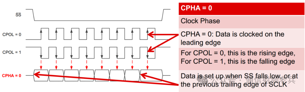 The second parameter, CPHA, determines at which clock phase the data is sampled. When CPHA is equal to 0, data is sampled on the leading edge of the clock pulse. When SS# (the active low form of the chip select signal) is pulled low, the first data bit is ready on the trailing edge of SCLK. When CPHA is equal to 1, data is sampled on the trailing edge of SCLK. In both clock phase modes, data is prepared on the previous clock edge.
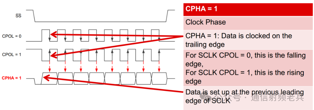 The combination of CPOL and CPHA allows SPI to have four operating modes. The table in this article shows SPI modes 0 to 3. Each mode defines different clock polarities and phases for SPI communication. Note that different SPI device and microcontroller manufacturers may have different definitions for SPI mode numbering. To determine clock polarity and phase information, refer to the data sheets of the controller and peripheral.
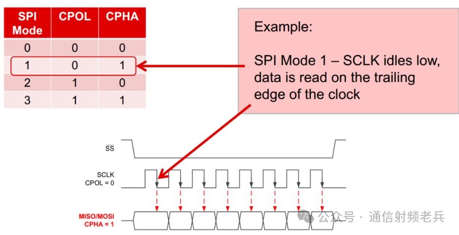
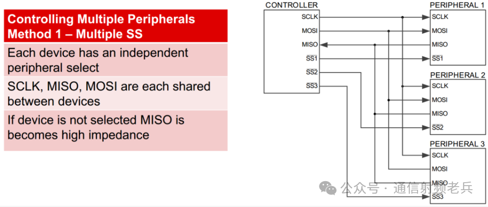
SPI can be used to communicate with multiple devices, which can be achieved in two different ways. First, since SPI uses slave select lines, the controller can communicate with multiple devices. Each peripheral receives its own slave select signal from the controller, while the remaining lines are shared.
When a device’s slave select line is selected, the remaining SPI lines are active. When the slave select line is not selected, the SPI lines are ignored. When not selected, each peripheral’s MOSI and SCLK lines are ignored, while each MISO line goes to a high-impedance state (Hi-Z), allowing the active peripheral to drive the MISO line without conflicting with other peripherals trying to drive the same line.
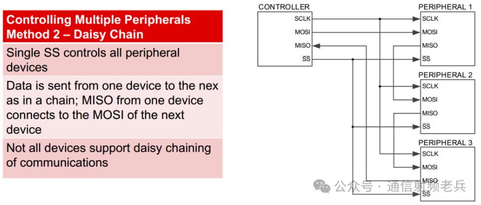
In some systems, a single SPI bus drives one peripheral, while other peripherals are connected in a daisy chain. In a daisy chain system, SCLK (serial clock) and slave select lines can be shared by all peripherals. However, the controller is only connected to a single MOSI (Master Out Slave In) line of the first peripheral. The MISO (Master In Slave Out) line of the first peripheral connects to the MOSI line of the next peripheral. This way, all peripherals connect from one MISO line to the next MOSI line, forming a chain.
For the last peripheral device, its MISO line connects to the controller. Data from all devices is passed through the chain and collected by the last peripheral. Not all devices can be controlled and read through daisy chain SPI connections. Devices must be specifically designed for this type of communication.
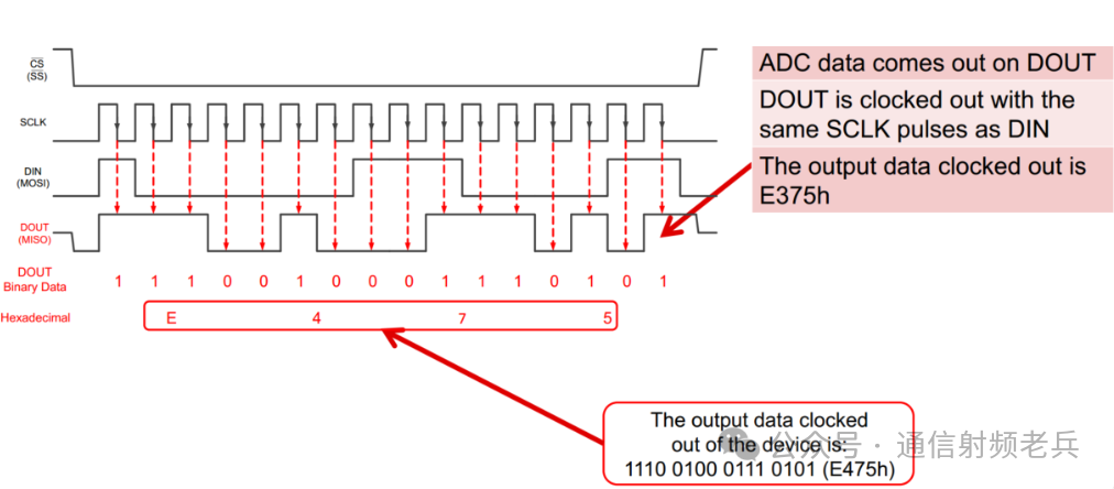
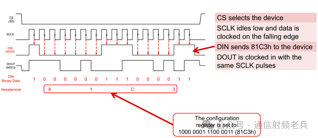
Below is an example of SPI data communication from a precision Analog-to-Digital Converter (ADC). This is a 16-bit ADC using SPI mode 1, where CPOL is equal to 0 and CPHA is equal to 1. In this case, SCLK is low in idle state, and data is input and output on the trailing edge of SCLK.
During a 16-bit data transfer cycle, two bytes of data are clocked into a configuration register. Simultaneously, 16 bits of ADC data are clocked out from the device. The ADC has a 16-bit configuration register, with settings as shown in the table. The values of these configuration registers will program the device to the settings described. In this example, we want to write the setting value of 81C3 (hexadecimal) to the device.
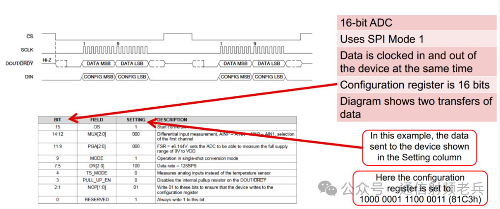
Continuing with the above ADC example, this is its 16-bit data transfer cycle, showing the state of the SPI lines. Again, SCLK is low in idle state, and data is transmitted on the falling edge of SCLK. Writing data to the device is accomplished through MOSI, or on this device, the corresponding pin is labeled DN. The configuration register is set to 81C3 (hexadecimal).
At the same time, data is clocked out from the ADC. Here, a random output data word is clocked out from the device. Observing the DOUT line, the output binary data is read as E476 (hexadecimal).