1. Computer Architecture
Before understanding computer architecture, let’s first get to know a few key figures who made significant contributions to the invention of computers.
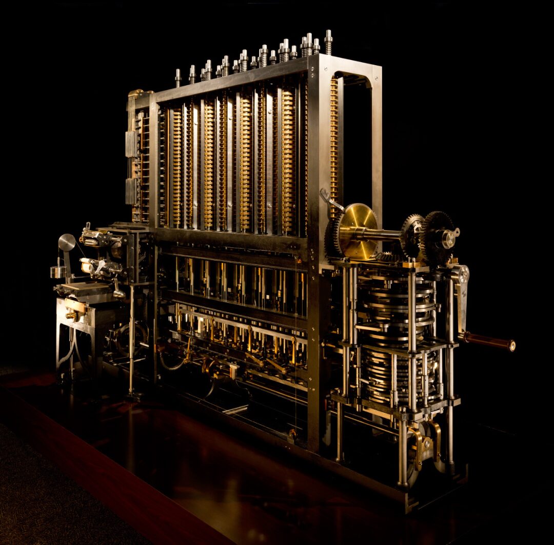
1. Charles Babbage
The father of the mechanical computer, a British nobleman, who built the first difference engine single-handedly, achieving a calculation precision of 6 decimal places. Later, he designed a 20-digit precision difference engine, and his design concepts have reached the pinnacle of mechanical design.
From 1985 to 1991, the London Science Museum successfully built Difference Engine No. 2 using pure 19th-century technology to commemorate the 200th anniversary of Babbage’s birth, based on his 1849 design.
Babbage is considered the most powerful brain of the last century, and his brain is preserved in the British Science Museum.
The grandmother of programmers, Ada Lovelace, proposed programming concepts such as loops and branches while working with Babbage, which we now take for granted.
2. Alan Turing
Known as the father of computer science and artificial intelligence. In 1931, Turing entered King’s College, Cambridge, and after graduation, pursued a Ph.D. at Princeton University in the U.S. After the outbreak of World War II, he returned to Cambridge and assisted the military in breaking the famous German code system Enigma, helping the Allies achieve victory in the war. Turing made numerous contributions to the development of artificial intelligence, proposing a test method to determine whether a machine possesses intelligence, known as the Turing Test, which still holds competitions every year.
The CO-LOSSUS machine, successfully developed by Turing’s wartime organization in 1943, employed some of the concepts proposed by Turing. It used 1,500 electronic tubes, a phototube reader, input via punched tape, and utilized bistable circuits to perform counting, binary arithmetic, and Boolean algebra logic operations. A total of 10 machines were produced, which excelled in code-breaking tasks.
I highly recommend the film “The Imitation Game,” based on Turing’s life, to experience the extraordinary life of this genius.

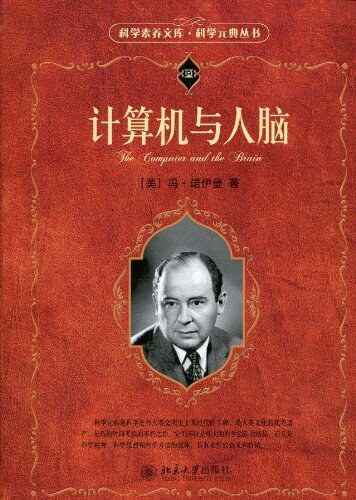
3. John von Neumann – “Computer and the Brain”
There are mainly two types of computer architecture: Harvard architecture and von Neumann architecture. Most modern computers are based on the von Neumann architecture.
I personally believe that von Neumann is the “smartest person of the last century, no exception.”
His personal achievements are numerous, and many are so complex that one might not even understand their names; only game theory is somewhat known.
This article only discusses the contributions of these giants to computers (in fact, computing was not von Neumann’s most significant achievement, and he did not spend much time and energy on computer research).
In October 1955, von Neumann was diagnosed with cancer. Almost at the last moment of his life, he wrote a lecture on the relationship between the human nervous system and computers on his deathbed. In 1958, his lecture was published under the title “Computer and the Brain.”
Von Neumann discussed the stimulation-response and memory issues of the nervous system from a mathematical perspective, mainly from the angles of logic and statistical mathematics, proposing that the nervous system has both digital and analog characteristics and exploring the control and logical structure of the nervous system.
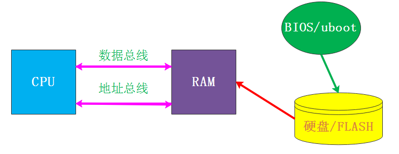
4. Von Neumann Architecture
The core of von Neumann is: “Stored Program, Sequential Execution”, which stipulates that a computer must have the following functions:
-
To send the required programs and data into the computer; -
Must have the ability to long-term memory of programs, data, intermediate results, and final computation results; -
To be able to perform various arithmetic, logical operations, and data transmission for data processing; -
To control the direction of the program as needed and coordinate the operation of various machine components according to instructions; -
To output the processing results to users as required.
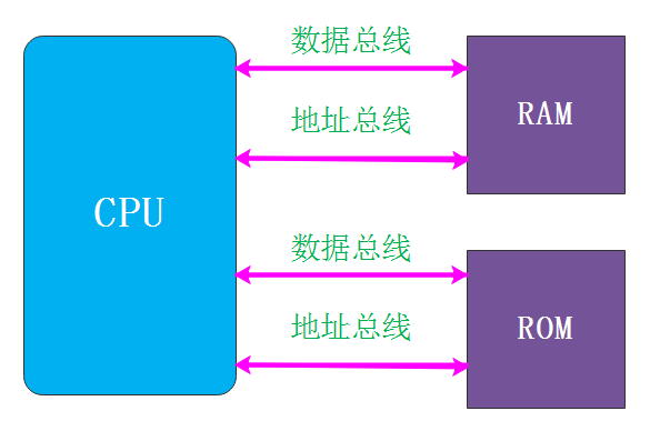
5. Harvard Architecture
The von Neumann architecture is different from the Harvard architecture.
The von Neumann architecture has both the program storage area and data storage that can be placed in memory with unified encoding, while the Harvard architecture has separate addressing.
6. Which Processors Are Harvard Architecture and von Neumann Architecture?
“Harvard Architecture”
MCUs (Microcontroller Units) are almost all based on Harvard architecture, such as the widely used 51 microcontroller and the typical STM32 microcontroller (core based on ARM Cortex-M series) which are all Harvard architecture.
“Von Neumann Architecture”
PCs and server chips (such as Intel and AMD), ARM Cortex-A series embedded chips (such as the Samsung Exynos-4412 with ARM Cortex-A9 core, Huawei’s Kirin 970 mobile chips, etc.) are all von Neumann architecture. These systems require a large amount of memory, so their working memory is DRAM, which is better suited for von Neumann systems.
“Hybrid Architecture”
In fact, modern CPUs (more accurately called SoCs) are not purely Harvard or von Neumann architecture, but rather hybrid architectures.
For example, the Samsung Exynos 4412, which uses the ARM Cortex-A9 core. The Exynos 4412 development board is equipped with 1024MB of DDR SDRAM and 8GB of eMMC.
During normal operation, all programs and data are loaded from eMMC to DDR, meaning that whether it is instructions or data, storage is in eMMC, and during execution, it is in DDR, and then sent to the CPU for processing through cache and registers. This is a typical von Neumann system.
However, the Exynos 4412 also has a certain capacity of 64KB iROM and 64KB iRAM, which are used for SoC booting and startup. After powering on the chip, it first executes the code stored in the internal iROM, making the 4412 behave like an MCU during this execution; iROM is like its flash, and iRAM is like its SRAM, which is again a typical Harvard architecture.
This is a hybrid design rather than a purely designed one. The reason for using a hybrid design is simply to leverage the strengths of both.
No matter if it’s a white cat or a black cat, a good cat is one that solves problems.
2. Computer Composition
Computer system = hardware system + software system. Hardware is the material foundation of the computer system, while software is the soul of the computer system. Hardware and software complement each other and form an inseparable whole.
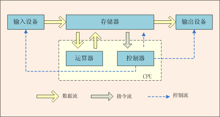
1). Input Devices
The task of input devices is to send the programs and raw data prepared by people into the computer and convert them into a format that the computer can recognize and accept internally. Commonly used devices include keyboards, mice, and scanners.
2). Output Devices
The task of output devices is to send the computer’s processing results in a form that can be accepted by people or other devices. Commonly used devices include monitors, printers, and plotters.
3). Memory, CPU
See Section 3.
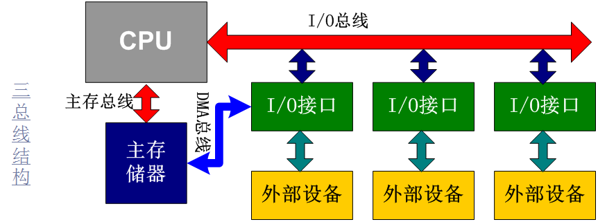
4). Computer Bus Structure
The basic components are connected in a certain way to form the hardware system of the computer.
The system bus includes three different functional buses: Data Bus DB, Address Bus AB, and Control Bus CB.
Data Bus DB is used to transmit data information. The bit width of the data bus is an important indicator of microcomputers, usually consistent with the word length of the microprocessor. For example, the Intel 8086 microprocessor has a word length of 16 bits, and its data bus width is also 16 bits.
Address Bus AB is specifically used to transmit addresses. The bit width of the address bus determines the size of the memory space that the CPU can directly address. For example, an 8-bit microcomputer with a 16-bit address bus can address a maximum space of 2^16 = 64KB, while a 16-bit microcomputer with a 20-bit address bus can address a space of 2^20 = 1MB.
Control Bus CB is used to transmit control signals and timing signals. Some control signals are sent from the microprocessor to the memory and I/O interface circuits, such as read/write signals, chip select signals, and interrupt response signals; others are feedback from other components to the CPU, such as interrupt request signals, reset signals, bus request signals, and ready signals. The specifics of the control bus depend on the CPU.
3. CPU Working Principle
The CPU mainly includes the arithmetic unit and the control unit.
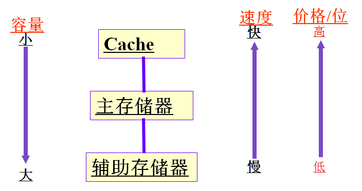
1) Memory
Memory is the component used to store programs and data; it is a memory device and the foundation for the computer to achieve “stored program control”.
Includes: Cache, main memory, auxiliary storage.
“Cache” is directly accessible by the CPU and is used to store the active parts of the currently executing program to quickly provide instructions and data to the CPU.
“Main Memory” is directly accessible by the CPU and is used to store the currently executing programs and data.
“Auxiliary Storage” is set outside the main unit and is not directly accessible by the CPU; it is used to store programs and data that are not currently running, which are transferred to main memory when needed.
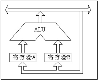
2) Arithmetic Unit
The core of the arithmetic unit is the Arithmetic Logic Unit (ALU), which also includes several registers (such as accumulator, temporary register, etc.).
The ALU can perform arithmetic operations (including basic operations such as addition and subtraction) and logical operations (including shifts, logical tests, or comparisons of two values). Compared to the control unit, the arithmetic unit acts according to the commands from the control unit, meaning that all operations performed by the arithmetic unit are directed by control signals from the control unit, so it is the executing component.
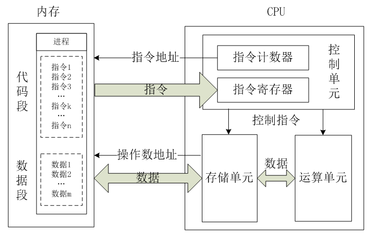
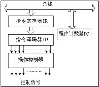
3) Control Unit
The control unit is the command and control center of the entire CPU, consisting of the Program Counter (PC), Instruction Register (IR), Instruction Decoder (ID), and Operation Controller (OC), which are crucial for coordinating the orderly operation of the entire computer.
It sequentially retrieves each instruction from memory based on the pre-programmed user instructions, places it in the Instruction Register (IR), decodes (analyzes) the instruction to determine what operation should be performed, and then sends micro-operation control signals to the corresponding components through the Operation Controller (OC) according to the determined timing. The Operation Controller (OC) mainly includes a pulse generator, control matrix, clock pulse generator, reset circuit, and start-stop circuit.
4) Summary of CPU Operation Principles
Under the influence of timing pulses, the control unit sends the instruction address pointed to by the instruction counter (this address is in memory) to the address bus, and then the CPU reads the instruction at this address into the instruction register for decoding.
For the data needed during the execution of the instruction, the data address is also sent to the address bus, and then the CPU reads the data into the internal storage unit (i.e., internal registers) for temporary storage, and finally commands the arithmetic unit to process the data.
This process continues to repeat.
5) Instruction Execution Process
The execution of an instruction typically includes the following four steps:
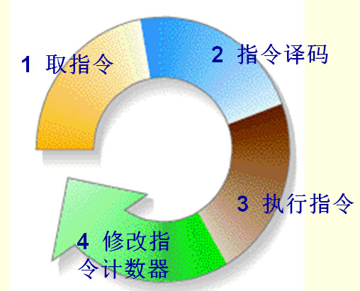
1. Fetch Instruction: The CPU’s control unit reads an instruction from memory and places it in the instruction register. 2. Decode Instruction: The instruction in the instruction register is decoded to determine what operation the instruction should perform (the operation code) and where the operand is located (the address of the operand). 3. Execute Instruction, divided into two phases: “Fetch Operand” and “Perform Operation.” 4. Modify the instruction counter to determine the address of the next instruction.
6) ARM Technical Features
The success of ARM is attributed to its unique corporate operation model and, of course, the excellent performance of ARM processors themselves. As an advanced RISC processor, ARM processors have the following characteristics:
-
Small size, low power consumption, low cost, high performance. -
Supports Thumb (16-bit) / ARM (32-bit) dual instruction sets, well compatible with 8-bit / 16-bit devices. -
Extensive use of registers, resulting in faster instruction execution. -
Most data operations are completed in registers. -
Flexible and simple addressing methods, high execution efficiency. -
Fixed instruction length. It’s necessary to explain the concept of RISC microprocessors and their differences from CISC microprocessors.
7) Development of ARM Architecture
Architecture is defined as the instruction set (ISA) and the programming model of processors based on this architecture. There can be multiple processors based on the same architecture, each with different performance and applications, but each processor’s implementation must adhere to this architecture. The ARM architecture provides high system performance for embedded system developers while maintaining excellent power consumption and efficiency.
The ARM architecture is steadily evolving to meet the general needs of ARM partners and design fields. Currently, the ARM architecture has defined eight versions, from version 1 to version 8. The functionality of the ARM instruction set has continuously expanded, and different series of ARM processors vary significantly in performance and application scope. However, if they share the same ARM architecture, the application software based on them is compatible.
Below, we briefly introduce the V7/V8 architecture.
v7 Architecture
The ARMv7 architecture was born out of the ARMv6 architecture. This architecture employs Thumb-2 technology, which has developed from ARM’s Thumb code compression technology while maintaining complete code compatibility with existing ARM solutions. Thumb-2 technology uses 31% less memory than pure 32-bit code, reducing system overhead while providing 38% higher performance than existing Thumb-based solutions. The ARMv7 architecture also adopts NEON technology, enhancing DSP and media processing capabilities nearly fourfold, and supports improved floating-point operations, meeting the needs of next-generation 3D graphics, gaming physics applications, and traditional embedded control applications.
v8 Architecture
The ARMv8 architecture is developed on the 32-bit ARM architecture and will be first used in product areas that require higher demands for extended virtual addresses and 64-bit data processing technologies, such as enterprise applications and high-end consumer electronics. The ARMv8 architecture includes two execution states: AArch64 and AArch32. The AArch64 execution state is aimed at 64-bit processing technology, introducing a new instruction set A64 that can access a large virtual address space; while the AArch32 execution state will support the existing ARM instruction set. Most features of the current ARMv7 architecture will be retained or further expanded in the ARMv8 architecture, such as TrustZone technology, virtualization technology, and NEON advanced SIMD technology.
8) ARM Microprocessor Architecture
The ARM core adopts a RISC architecture. The main features of the ARM architecture are as follows:
-
Utilizes a large number of registers, all of which can be used for various purposes. -
Employs a Load/Store architecture. -
Each instruction is conditionally executed. -
Uses multi-register Load/Store instructions. -
Can complete a normal shift operation and a normal ALU operation within a single clock cycle. -
Extends the ARM instruction set through coprocessor instructions, including new registers and data types in the programming mode. -
If the Thumb instruction set is also considered part of the ARM architecture, then the Thumb architecture can also represent the instruction set in a high-density 16-bit compressed form.
9) ARM Instructions
ARM instructions are RISC (Reduced Instruction Set Computing), focusing on simplifying the structure of computers and increasing processing speed. RISC selects the most frequently used simple instructions, discarding complex instructions, fixing instruction lengths, reducing instruction formats and addressing methods, and minimizing or eliminating microcode control. These features make RISC particularly suitable for embedded processors.
RISC can achieve extremely fast microprocessors with relatively few transistors. Research shows that only about 20% of instructions are the most commonly used. Reducing the number of instructions that the processor can execute to a minimum and optimizing their execution can significantly improve processing speed.
Generally speaking, RISC processors are 50%-75% faster than equivalent CISC (Complex Instruction Set Computer) processors, and RISC processors are also easier to design and debug.
The general instruction format is as follows:

“Opcode:” The opcode refers to the assembly language symbols like mov, add, jmp, etc.;
“Operand Address:” This indicates where the operand required by the instruction is located, whether in memory or in the CPU’s internal registers.
The actual machine instruction format is far more complex than this; the following diagram shows the common ARM instruction format:
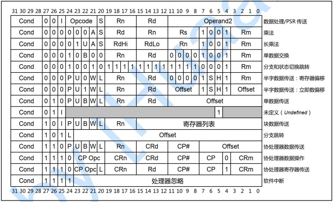
Regarding these machine instruction formats, we will analyze a few of them later. For most of our readers, there is no need to spend too much effort studying these machine instructions; a general understanding is sufficient.
Understanding the CPU from a macro perspective is sufficient at this stage; we will gradually move into subsequent learning stages, introducing ARM register modes, exceptions, addressing, assembly instructions, and the writing of assembly language embedded in C code.
4. SoC
SoC: A System on Chip integrates a computer or other electronic systems into a single chip. A system on chip can process digital signals, analog signals, mixed signals, and even higher frequency signals.
Narrowly speaking, it integrates the core chip of information systems, integrating key components of the system onto a single chip; broadly speaking, SoC is a miniature system. If the CPU is the brain, then SoC includes the brain, heart, eyes, and hands.
1. ARM-based SoC
System on chips are often required in embedded systems. The integration scale of SoCs is large, typically reaching millions to tens of millions of gates. SoCs are relatively flexible, allowing the integration of ARM architecture processors with specialized peripheral chips to form a system.
The following diagram shows a typical ARM-based SoC architecture.
A typical ARM-based SoC architecture usually includes the following main components:
-
ARM Processor Core -
Clocks and Reset Controller -
Interrupt Controller -
ARM Peripherals -
GPIO -
DMA Port -
External Memory Interface -
On-chip RAM -
AHB, APB Bus
Some ARM processors, such as Hisi-3507, Exynos-4412, etc., are SoC systems, especially application processors that integrate many peripheral devices, providing strong support for executing more complex tasks and applications.
This architecture is the cornerstone for understanding assembly instructions and writing bare-metal programs.
When we obtain a new SoC’s datasheet, we first need to check the SoC’s “RAM space, clock frequency, which external device controllers are included, the operating principles of each peripheral controller, the pin multiplexing of each peripheral to GPIO, the SFR addresses of each controller, how the interrupt controller manages numerous interrupt sources, etc.”
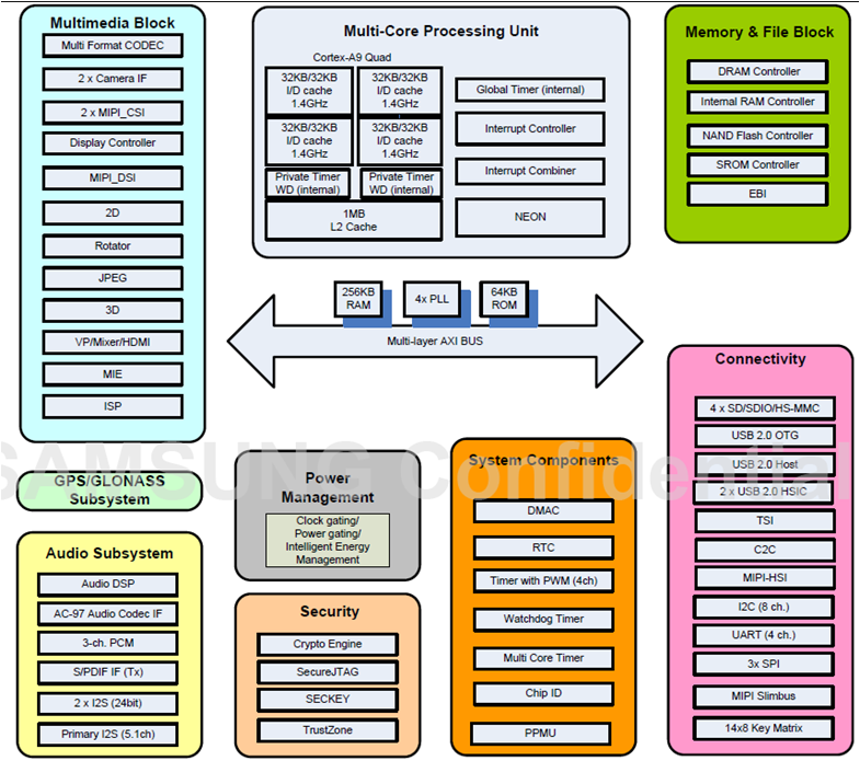
2. Samsung Exynos 4412
In early 2012, Samsung officially launched its first quad-core mobile processor, the Exynos 4412.
The following is the SoC structure diagram of Samsung’s Exynos 4412.

As shown in the figure above, the Exynos 4412 mainly includes the following modules:
-
4 (quad) Cortex-A9 processors -
1MB L2 Cache -
Interrupt Controller, managing all interrupt sources -
Interrupt Combiner, managing some interrupt sources within the SoC -
NEON ARM architecture processor extension structure, aimed at enhancing multimedia (video/audio) encoding/decoding, user interface, 2D/3D graphics, and gaming to improve multimedia experiences -
DRAM, Internal RAM, NAND Flash, SROM Controller for various storage devices -
SDIO, USB, I2C, UART, SPI buses -
RTC, Watchdog Timer -
Audio Subsystem -
IIS (Integrated Interface of Sound), integrated voice interface -
Power Management -
Multimedia Block
This new Exynos quad-core processor features a 32nm HKMG (High-K Metal Gate) process, supporting dual-channel LPDDR2 1066. Samsung has increased the graphics processor frequency from the previous 266MHz to 400MHz, indicating a 60% overall performance boost compared to existing dual-core models, and a 50% improvement in image processing capabilities.
The Samsung Galaxy S III smartphone uses the Exynos 4412 processor.