The Serial Peripheral Interface (SPI) is one of the most widely used interfaces between microcontrollers and peripheral ICs such as sensors, ADCs, DACs, shift registers, and SRAM.
SPI is a synchronous, full-duplex, master-slave interface. Data from the master or slave is synchronized on the rising or falling edge of the clock. Both the master and slave can transmit data simultaneously. The SPI interface can be either 3-wire or 4-wire. This article focuses on the commonly used 4-wire SPI interface.
Interface
The 4-wire SPI device has four signals:
-
Clock (SPICLK, SCLK)
-
Chip Select (CS) Master Output
-
Slave Input (MOSI) Master Input
-
Slave Output (MISO)
The device that generates the clock signal is called the master. The data transmitted between the master and slave is synchronized with the clock generated by the master. Compared to the I2C interface, SPI devices support higher clock frequencies. Users should refer to the product datasheet for the clock frequency specifications of the SPI interface.
There can only be one master in an SPI interface, but there can be one or more slaves. Figure 1 shows the SPI connection between the master and slave.
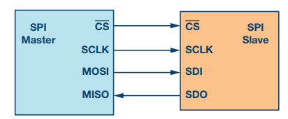
Figure 1. SPI Configuration with Master and Slave
The chip select signal from the master is used to select the slave. This is usually a low-level active signal, which disconnects the slave from the SPI bus when pulled high. When using multiple slaves, the master needs to provide a separate chip select signal for each slave. The chip select signal in this article is always a low-level active signal.
MOSI and MISO are the data lines. MOSI sends data from the master to the slave, while MISO sends data from the slave to the master.
Data Transmission
To start SPI communication, the master must send a clock signal and select the slave by enabling the CS signal. The chip select is typically a low-level active signal. Therefore, the master must send a logic 0 on this signal to select the slave. SPI is a full-duplex interface, allowing the master and slave to send data simultaneously over the MOSI and MISO lines. During SPI communication, data transmission (serially shifting out to the MOSI/SDO line) and reception (sampling or reading data on the MISO/SDI line) occur simultaneously. The serial clock edge synchronizes the shifting and sampling of data. The SPI interface allows users to flexibly choose the rising or falling edge of the clock to sample and/or shift data. To determine the number of bits transmitted using the SPI interface, refer to the device datasheet.
Clock Polarity and Clock Phase
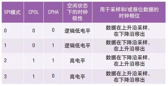
In SPI, the master can choose the clock polarity and clock phase. The CPOL bit sets the polarity of the clock signal during the idle state. The idle state refers to the period when CS is high at the start of transmission and transitions to low, and when CS is low at the end of transmission and transitions to high. The CPHA bit selects the clock phase. Depending on the state of the CPHA bit, data can be sampled and/or shifted on the rising or falling edge of the clock. The master must select the clock polarity and clock phase according to the requirements of the slave. Based on the selection of CPOL and CPHA bits, four SPI modes are available. Table 1 shows these four SPI modes.
Table 1. SPI Modes Selected by CPOL and CPHA
Figures 2 to 5 show communication examples in the four SPI modes. In these examples, the data is displayed on the MOSI and MISO lines. The start and end of the transmission are indicated by green dashed lines, the sampling edges by orange dashed lines, and the shifting edges by blue dashed lines. Note that these diagrams are for reference only. To successfully perform SPI communication, users must refer to the product datasheet and ensure compliance with the device’s timing specifications.
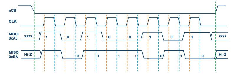
Figure 2. SPI Mode 0, CPOL = 0, CPHA = 0: CLK Idle State = Low, Data Sampled on Rising Edge, and Shifted Out on Falling Edge
Figure 3 shows the timing diagram for SPI Mode 1. In this mode, the clock polarity is 0, indicating that the idle state of the clock signal is low. The clock phase in this mode is 1, indicating that data is sampled on the falling edge (shown by the orange dashed line) and shifted out on the rising edge of the clock signal (shown by the blue dashed line).
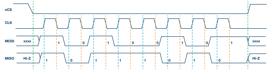
Figure 3. SPI Mode 1, CPOL = 0, CPHA = 1: CLK Idle State = Low, Data Sampled on Falling Edge, and Shifted Out on Rising Edge
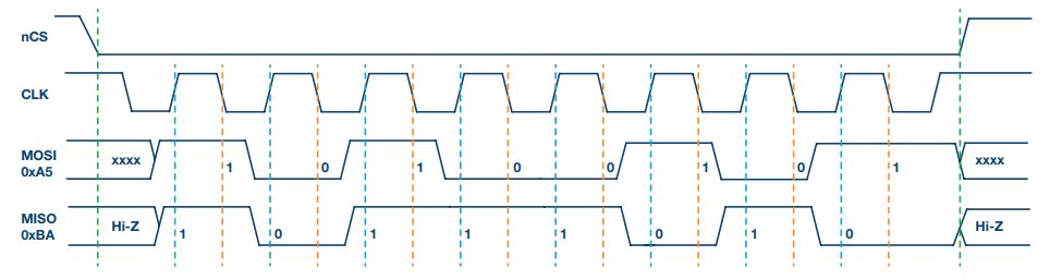
Figure 4. SPI Mode 2, CPOL = 1, CPHA = 1: CLK Idle State = High, Data Sampled on Falling Edge, and Shifted Out on Rising Edge
Figure 4 shows the timing diagram for SPI Mode 2. In this mode, the clock polarity is 1, indicating that the idle state of the clock signal is high. The clock phase in this mode is 1, indicating that data is sampled on the falling edge (shown by the orange dashed line) and shifted out on the rising edge of the clock signal (shown by the blue dashed line).
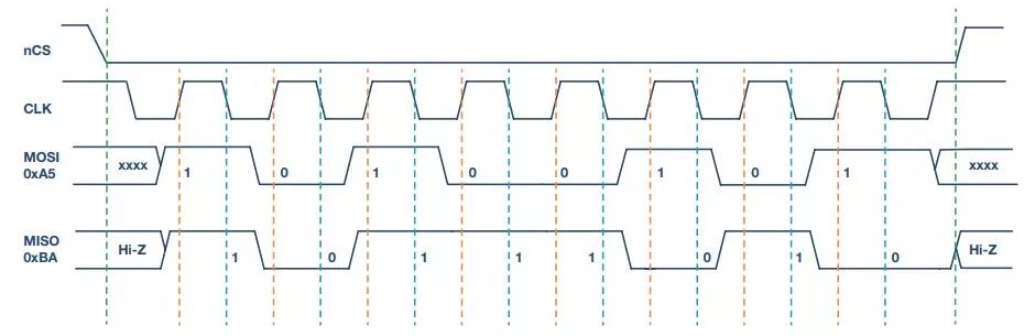
Figure 5. SPI Mode 3, CPOL = 1, CPHA = 0: CLK Idle State = High, Data Sampled on Rising Edge, and Shifted Out on Falling Edge
Figure 5 shows the timing diagram for SPI Mode 3. In this mode, the clock polarity is 1, indicating that the idle state of the clock signal is high. The clock phase in this mode is 0, indicating that data is sampled on the rising edge (shown by the orange dashed line) and shifted out on the falling edge of the clock signal (shown by the blue dashed line).
Multi-Slave Configuration
Multiple slaves can be used with a single SPI master. Slaves can be connected in a conventional mode or in a daisy chain mode.
Conventional SPI Mode
In conventional mode, the master needs to provide a separate chip select signal for each slave. Once the master enables (pulls low) the chip select signal, the clock and data on the MOSI/MISO lines become available for the selected slave. If multiple chip select signals are enabled, the data on the MISO line will be corrupted because the master cannot identify which slave is transmitting data.
As shown in Figure 6, as the number of slaves increases, the number of chip select lines from the master also increases. This rapidly increases the number of inputs and outputs that the master needs to provide, limiting the number of slaves that can be used. Other techniques can be used to increase the number of slaves in conventional mode, such as using multiplexers to generate chip select signals.
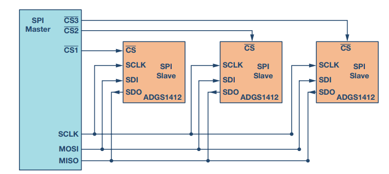
Figure 6. Multi-Slave SPI Configuration
Daisy Chain Mode
In daisy chain mode, all slave chip select signals are connected together, and data propagates from one slave to the next. In this configuration, all slaves receive the same SPI clock simultaneously. Data from the master is sent directly to the first slave, which then provides the data to the next slave, and so on.
When using this method, the number of clock cycles required to transmit data is proportional to the position of the slave in the daisy chain. For example, in the 8-bit system shown in Figure 7, to enable the third slave to receive data, 24 clock pulses are needed, while only 8 clock pulses are required in conventional SPI mode.
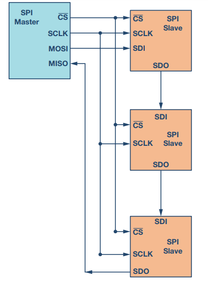
Figure 7. Multi-Slave SPI Daisy Chain Configuration
Figure 8 shows the clock cycles and data propagation through the daisy chain. Not all SPI devices support daisy chain mode. Please refer to the product datasheet to confirm if daisy chaining is available.
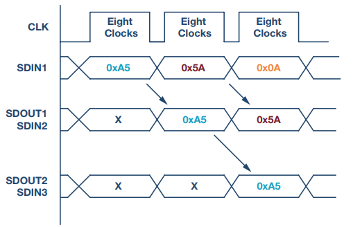
Figure 8. Daisy Chain Configuration: Data Propagation
ADI’s SPI-Compatible Analog Switches and Multiplexers
ADI’s latest generation of SPI-compatible switches can significantly save space without compromising precision switch performance. This section of the article will discuss a case study illustrating how SPI-compatible switches or multiplexers can greatly simplify system-level design and reduce the number of required GPIOs.
The ADG1412 is a four-channel, single-pole single-throw (SPST) switch that requires four GPIOs connected to the control inputs of each switch. Figure 9 shows the connection between a microcontroller and an ADG1412.
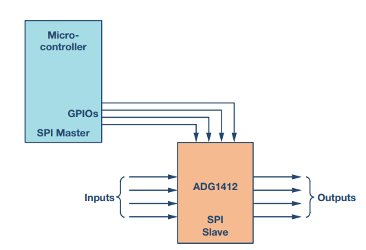
Figure 9. Microcontroller GPIOs Used as Control Signals for Switches
As the number of switches on the circuit board increases, the number of required GPIOs also increases significantly. For example, when designing a test instrument system, a large number of switches are used to increase the number of channels in the system. In a 4×4 crosspoint matrix configuration, four ADG1412s are used. This system requires 16 GPIOs, limiting the available GPIOs in a standard microcontroller. Figure 10 shows the connection of four ADG1412s using 16 GPIOs from a microcontroller.
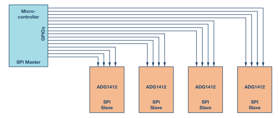
Figure 10. Significant Increase in Required GPIOs in Multi-Slave Configuration
How to Reduce the Number of GPIOs?
One method is to use a serial-to-parallel converter, as shown in Figure 11. The parallel signals output by this device can be connected to the control inputs of the switches, and the device can be configured via the SPI serial interface. The downside of this method is that the additional device increases the bill of materials.
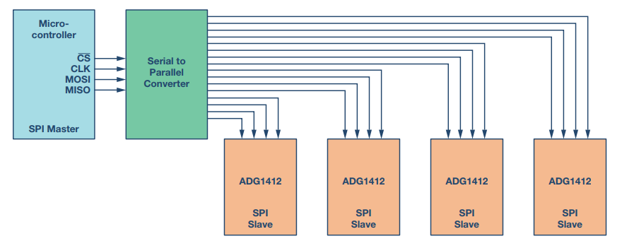
Figure 11. Multi-Slave Switches Using Serial-to-Parallel Converter
Another method is to use SPI-controlled switches. The advantage of this method is that it reduces the number of required GPIOs and eliminates the overhead of an additional serial-to-parallel converter. As shown in Figure 12, instead of needing 16 microcontroller GPIOs, only 7 microcontroller GPIOs are required to provide SPI signals to four ADGS1412s. The switches can be configured in a daisy chain to further optimize the number of GPIOs. In a daisy chain configuration, regardless of how many switches the system uses, only four GPIOs from the master (microcontroller) are used.
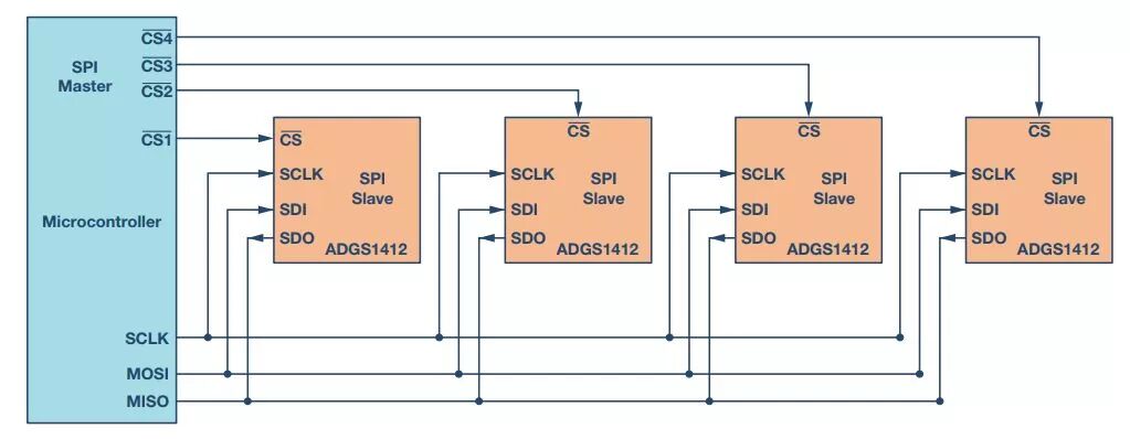
Figure 12. SPI-Compatible Switches Save Microcontroller GPIOs
Figure 13 is for illustration purposes. The ADGS1412 datasheet recommends using a pull-up resistor on the SDO pin. For simplicity, this example uses four switches. As the number of switches in the system increases, the advantages of a simpler circuit board and space savings become important.
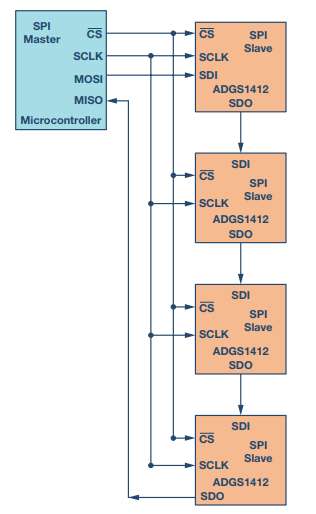
Figure 13. SPI Switches in Daisy Chain Configuration Further Optimize GPIOs
Placing eight four-channel SPST switches on a 6-layer circuit board in a 4×8 crosspoint configuration, ADI’s SPI-compatible switches can save 20% of the total circuit board space.