Follow “Wireless Technology Alliance”for valuable IoT market insights and the latest technical analyses
1. Introduction
This article extracts the RF architecture of the CC2640R2F chip from the metal layer images at the 7th, 6th, 4th, and 3rd layers under an electron microscope. The extracted features include the layout characteristics of RF, such as high-speed signal routing, inductors, and AC coupling capacitors (the details and functions of circuits implemented in the second metal or lower metal layers are not extracted, along with the layout of receiving and transmitting signals between the digital processor core and the data converter). This analysis focuses on the RF architecture, without analyzing the digital core or other analog functions unrelated to RF (such as voltage regulators, DC sources, reference REF generators, PLL, and test overhead).
2. Chip Overview
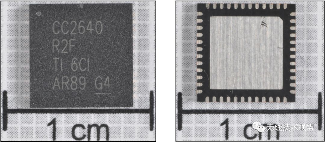
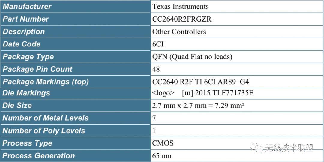
Let’s first look at the basic information of the CC2640R2F Bluetooth chip, which is manufactured using a 65nm CMOS process, with a die size of 7.29mm (2.66mm x 2.66mm), and is packaged in a 7×7 48-pin VQFN form.
Basic Information of the Chip
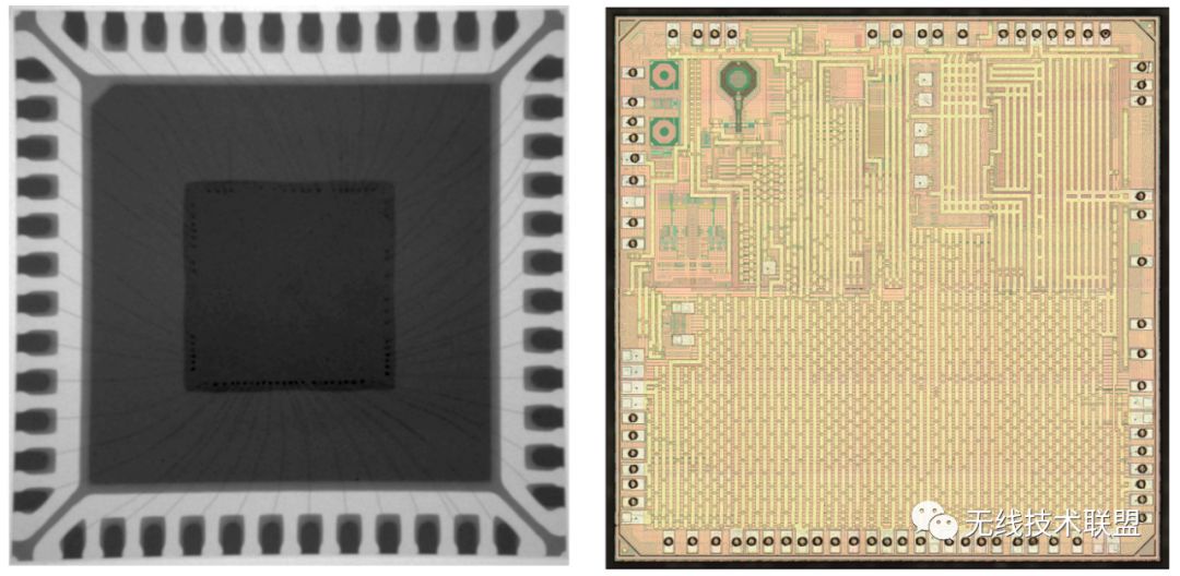
Physical Image of the Chip under X-ray and Microscope
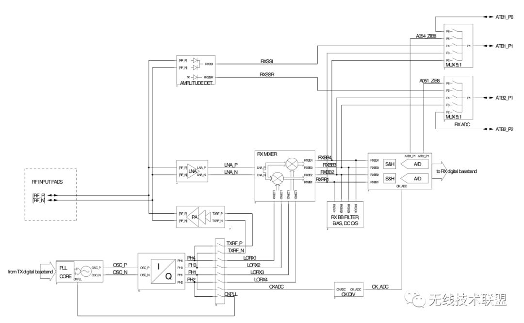
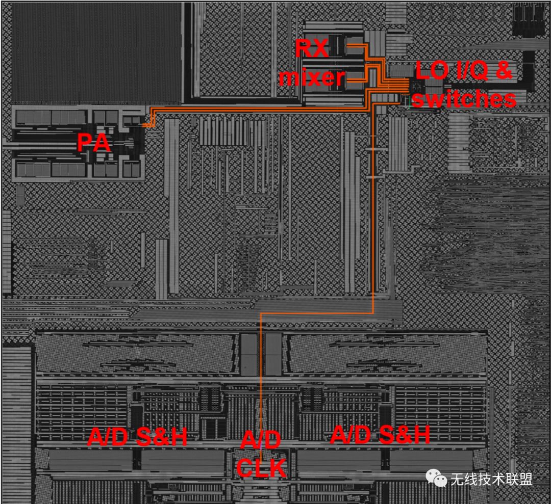
Opening the chip, the Bluetooth transceiver is located at the upper left corner of the CC2640R2F chip.The RF signal pins connect to the bonding pads [RF_P] and [RF_N] at the upper left corner.The RF signal connects to three modules:1) LNA, including two matched unbalanced inductors;2) Inductor-less Power Amplifier (PA);3) Amplitude Detector.The LNA signal is directly connected to the receiving end of the downconverter mixer, which is located near the PLL oscillator that also generates the modulated RF signal for the PA.
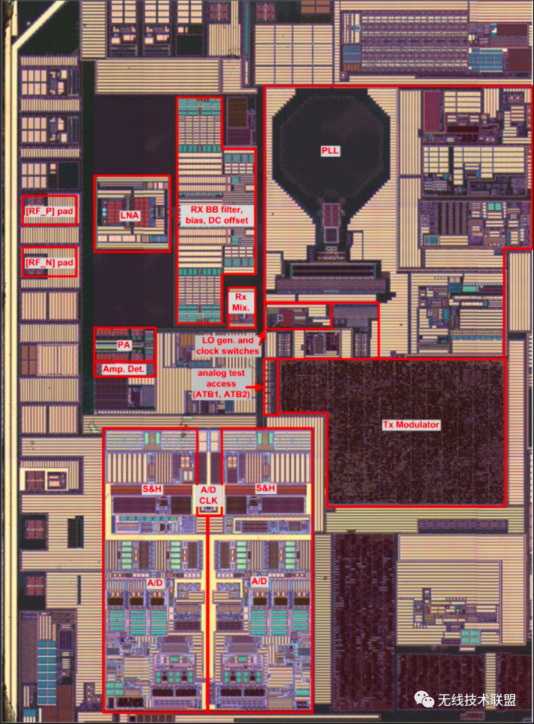
RF_P, FR_N, LNA, PA signal routing is shown in the figure.

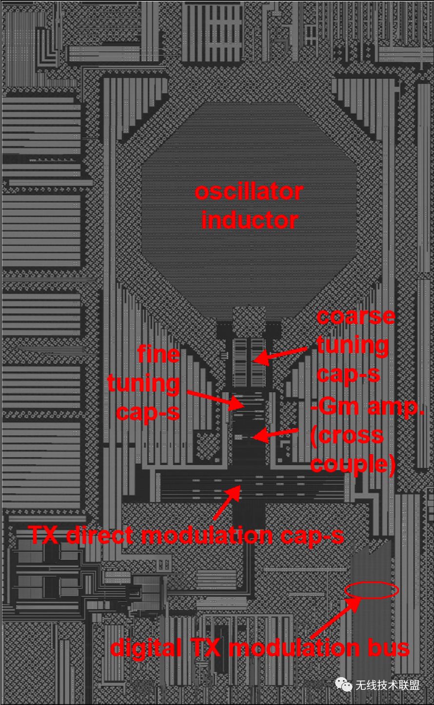
The layout of the PLL is shown in the following figure, and this oscillator is wound with LC inductors.
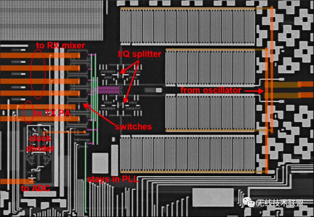
The oscillator signal is divided to output multiple orthogonal clock signals, and the clock source output is as follows:
1) RX oscillator signal;
2) TX modulated RF signal;
3) General clock signals, one for the Analog-to-Digital Converter (A/D), and another for PLL feedback;
Clock Source
The following photo shows the clock wiring from the PLL to various destinations.
Clock Signal Distribution
Although the TX baseband signal wiring is completely submerged in the digital domain and cannot be identified, the downconverted orthogonal RX signal wiring can be seen traversing the entire analog area, potentially connecting to the RX mixer in the first or second metal layer.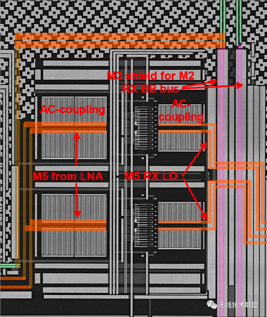
RX Mixing
The following figure shows the RX baseband signal routing.The large symmetric circuit in the upper half includes large resistors and capacitor arrays, as well as active circuits.The balanced layout suggests that this module may contain some filtering circuits and DC sources with bias.
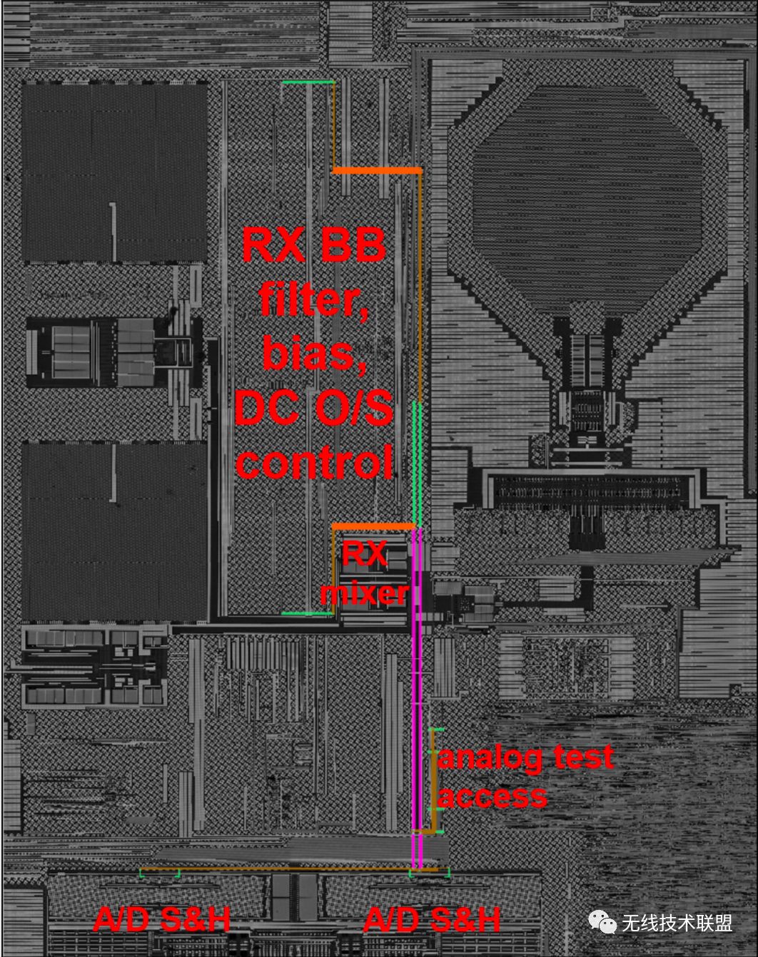
RX Analog Baseband Wiring
The endpoint of the RX baseband signal is a pair of A/D converters, whose digital outputs are unrecognized.
The transmitting PA is located below the LNA.The following figure shows its view in the third metal layer.
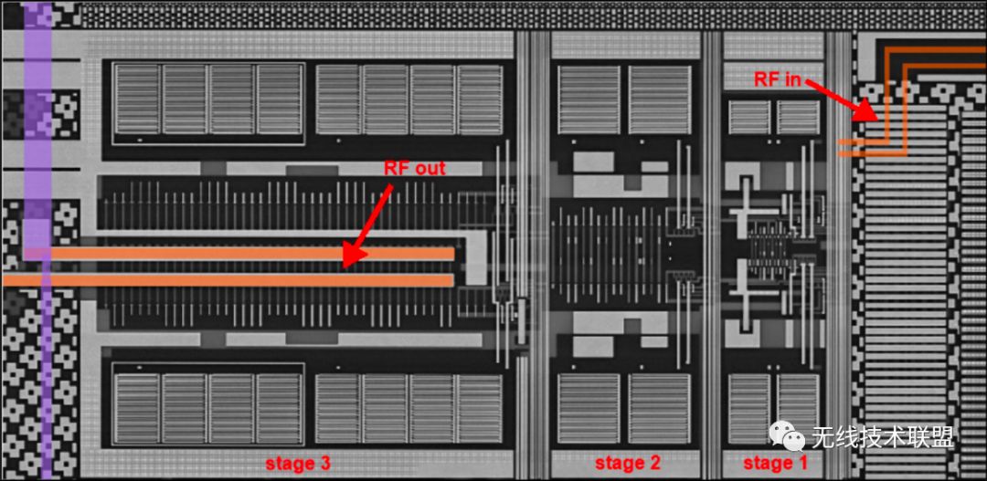
TX Amplifier
The amplitude detector is shown in the following figure, where the RF signal is AC coupled to this circuit. The RX baseband signal, the amplitude detector output signal, and two signals from the A/D converter are connected to a set of switches, which may be used for testing.
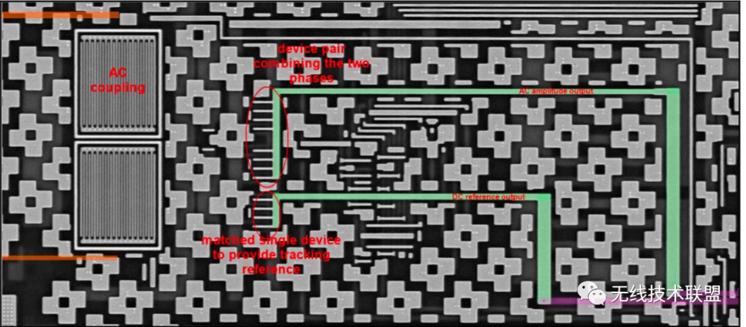
Amplitude Detector
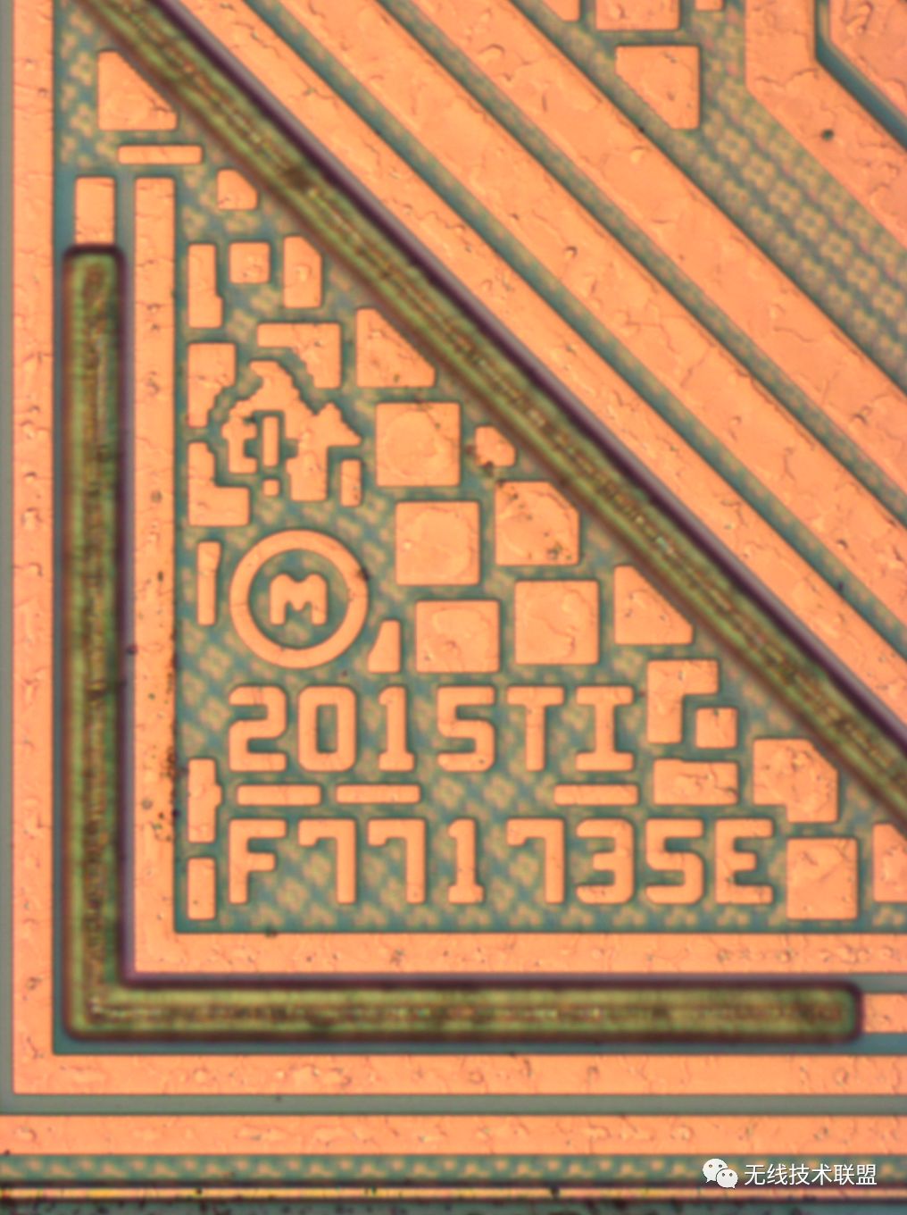
Finally, here is a logo image on the chip, wishing everyone a prosperous start to work!
Industry Layout of Low Power Bluetooth Leader from Nordic Financial Report
Layout Behind Dialog’s $0.5 BLE Chip DA14531
Origins of BLE RF Spurious Sources and Common Handling Methods
Apple’s New Phone Subtly Integrates UWB Technology, Can Consumer UWB Technology Rise?
Discussing Strategies for Selecting Low Power Wireless SoC Chips