Click the image to learn more
Preface
Chapter 1 Advanced Packaging 1
1.1 Introduction 1
1.2 Applications of Semiconductors 1
1.3 Driving Forces of System Technology 1
1.3.1 AI 1
1.3.2 5G 2
1.4 Overview of Advanced Packaging 3
1.4.1 Types of Advanced Packaging 3
1.4.2 Levels of Advanced Packaging 3
1.5 2D Fan-out (First Die Up) IC Integration 5
1.6 2D Flip Chip IC Integration 5
1.7 PoP, SiP, and Heterogeneous Integration 6
1.8 2D Fan-out (Last Die Up) IC Integration 8
1.9 2.1D Flip Chip IC Integration 8
1.10 2.1D Flip Chip IC Integration with Interconnect Bridges 9
1.11 2.1D Fan-out IC Integration with Interconnect Bridges 9
1.12 2.3D Fan-out (First Die Up) IC Integration 10
1.13 2.3D Flip Chip IC Integration 10
1.14 2.3D Fan-out (Last Die Up) IC Integration 11
1.15 2.5D (Solder Bump) IC Integration 12
1.16 2.5D (Micro Bump) IC Integration 12
1.17 Micro Bump 3D IC Integration 13
1.18 Micro Bump Chiplet 3D IC Integration 14
1.19 No Bump 3D IC Integration 14
1.20 No Bump Chiplet 3D IC Integration 15
1.21 Summary and Recommendations 15
References 16
Chapter 2 System-in-Package 22
2.1 Introduction 22
2.2 System on Chip 22
2.3 Overview of SiP 23
2.4 Purpose of Using SiP 23
2.5 Practical Applications of SiP 23
2.6 Examples of SiP 24
2.7 SMT 25
2.7.1 PCB 26
2.7.2 SMD 28
2.7.3 Solder Paste 29
2.7.4 Stencil Printing of Solder Paste and Automated Optical Inspection 30
2.7.5 Pick and Place of SMD 32
2.7.6 AOI of SMD on PCB 33
2.7.7 SMT Solder Reflow 33
2.7.8 AOI and X-ray Inspection of Defects 34
2.7.9 Rework 35
2.7.10 Summary and Recommendations 36
2.8 Flip Chip Technology 36
2.8.1 Wafer Bump Formation Technology Based on Stencil Printing 37
2.8.2 C4 Wafer Bump Formation Technology 38
2.8.3 C2 Wafer Bump Formation Technology 40
2.8.4 Flip Chip Assembly – C4/C2 Bump Mass Reflow (CUF) 40
2.8.5 Bottom Fill to Enhance Reliability 42
2.8.6 Flip Chip Assembly – Low Pressure Thermal Compression Bonding of C4/C2 Bumps (CUF) 44
2.8.7 Flip Chip Assembly – High Pressure Thermal Compression Bonding of C2 Bumps (NCP) 45
2.8.8 Flip Chip Assembly – High Pressure Thermal Compression Bonding of C2 Bumps (NCF) 45
2.8.9 An Advanced Flip Chip Assembly – C2 Bump Liquid Phase Contact Thermal Compression Bonding 47
2.8.10 Summary and Recommendations 53
References 54
Chapter 3 Fan-In Wafer-Level/Board-Level Chip Scale Packaging 63
3.1 Introduction 63
3.2 Fan-In Wafer-Level Chip Scale Packaging (WLCSP) 65
3.2.1 Packaging Structure 65
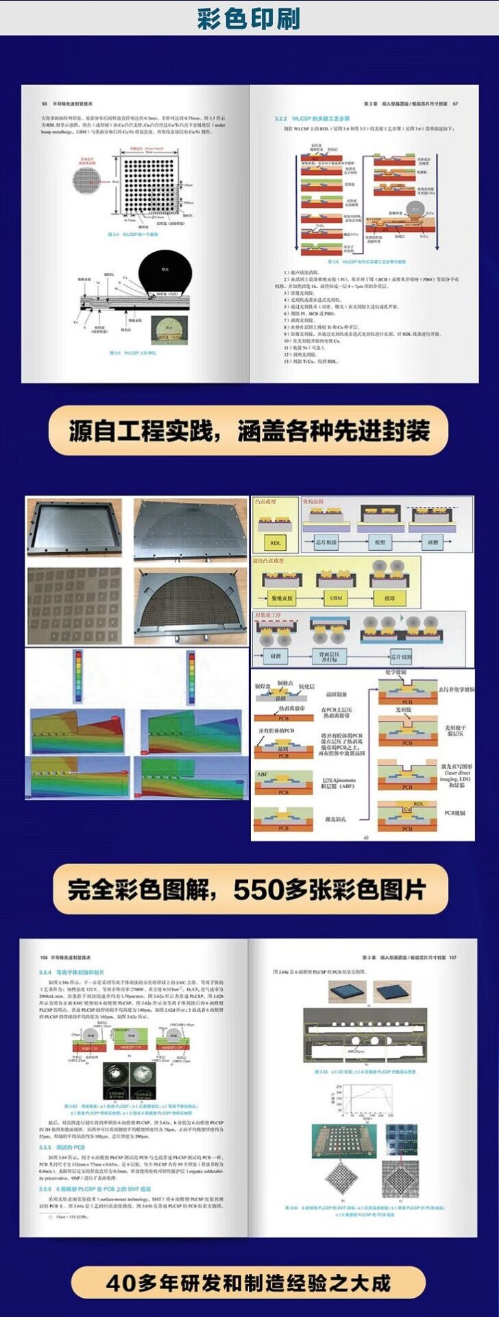
3.2.2 Key Process Steps of WLCSP 67
3.2.3 Assembly of WLCSP on PCB 68
3.2.4 Thermal Simulation of WLCSP Assembly on PCB 68
3.2.5 Summary and Recommendations 74
3.3 Fan-In Board-Level Chip Scale Packaging (PLCSP) 75
3.3.1 Test Chip 75
3.3.2 Test Packaging 76
3.3.3 PLCSP Process Flow 77
3.3.4 PLCSP Assembly on PCB 83
3.3.5 Drop Test of PLCSP Assembly on PCB 84
3.3.6 Thermal Cycling Test of PLCSP Assembly on PCB 86
3.3.7 Thermal Cycling Simulation of PLCSP Assembly on PCB 92
3.3.8 Summary and Recommendations 95
3.4 Six-Sided Molding Wafer-Level Chip Scale Packaging 96
3.4.1 Startech’s eWLCSP 97
3.4.2 United Technology’s WLCSP 97
3.4.3 SPIL’s mWLCSP 97
3.4.4 Huatian Technology’s WLCSP 99
<3.4.5 SPIL and MediaTek’s mWLCSP 99
3.4.6 Summary and Recommendations 102
3.5 Six-Sided Molding Board-Level Chip Scale Packaging 102
3.5.1 Structure of Six-Sided Molding PLCSP 102
3.5.2 Front Wafer Cutting and EMC Molding 104
3.5.3 Back Thinning and Wafer Back Molding 104
3.5.4 Plasma Etching and Dicing 106
3.5.5 Test PCB 106
3.5.6 SMT Assembly of Six-Sided Molding PLCSP on PCB 106
3.5.7 Thermal Cycling Test of Six-Sided Molding PLCSP 108
3.5.8 Thermal Cycling Simulation of Six-Sided Molding PLCSP Assembly on PCB 111
3.5.9 Summary and Recommendations 115
References 115
Chapter 4 Fan-Out Wafer-Level/Board-Level Packaging 124
4.1 Introduction 124
4.2 Fan-Out (First Die Up, Face Down) Wafer-Level Packaging (FOWLP) 125
4.2.1 Test Chip 125
4.2.2 Test Packaging 126
4.2.3 Traditional First Die Up (Face Down) Wafer-Level Process 127
4.2.4 New Processes for Heterogeneous Integration Packaging 128
4.2.5 Dry Film EMC Lamination 128
4.2.6 Temporary Bonding to Another Glass Support 128
4.2.7 Redistribution Layer 130
4.2.8 Solder Ball Placement 131
4.2.9 Final Debonding 131
4.2.10 PCB Assembly 134
4.2.11 Reliability of Heterogeneous Integration (Drop Test) 135
4.2.12 Summary and Recommendations 137
4.3 Fan-Out (First Die Up, Face Down) Board-Level Packaging (FOPLP) 137
4.3.1 Heterogeneous Integration of Test Packaging 138
4.3.2 A New Uni-SIP Process 140
4.3.3 Dry Film Lamination of ECM Panel 140
4.3.4 Lamination of Uni-SIP Structure 141
4.3.5 New ABF Lamination, Laser Drilling, and De-bonding 141
4.3.6 Laser Direct Writing Patterns and PCB Copper Plating 144
4.3.7 Summary and Recommendations 145
4.4 Fan-Out (First Die Up, Face Up) Wafer-Level Packaging 146
4.4.1 Test Chip 146
4.4.2 Process Flow 146
4.5 Fan-Out (First Die Up, Face Up) Board-Level Packaging 148
4.5.1 Packaging Structure 148
4.5.2 Process Flow 148
4.6 Fan-Out (Last Die Up or First RDL) Wafer-Level Packaging 150
4.6.1 IME’s First RDL FOWLP 151
4.6.2 Test Structure 151
4.6.3 Key Process Steps of First RDL 152
4.6.4 PCB Assembly of First RDL FOWLP 154
4.7 Fan-Out (Last Die Up or First RDL) Board-Level Packaging 154
4.7.1 Test Chip 154
4.7.2 Test Packaging 154
4.7.3 Heterogeneous Integration for First RDL Board-Level Packaging 157
4.7.4 RDL Substrate Manufacturing 157
4.7.5 Wafer Bump Formation 160
4.7.6 Chip-Substrate Bonding 160
4.7.7 Bottom Fill and EMC Molding 162
4.7.8 Panel/Strip Transfer 163
4.7.9 Opening of Solder Mask and Surface Treatment 163
4.7.10 Ball Placement, Debonding, and Strip Cutting 163
4.7.11 PCB Assembly of First RDL Board-Level Packaging 165
4.7.12 Drop Test Results and Failure Analysis 165
4.7.13 Thermal Cycling Test Results and Failure Analysis 169
4.7.14 Thermal Cycling Simulation 174
4.7.15 Summary and Recommendations 175
4.8 Mini-LED RGB Display Fan-Out Board-Level Packaging 176
4.8.1 Test mini-LED 177
4.8.2 SMD Packaging of Mini-LED RGB Display 178
4.8.3 RDL and Mini-LED RGB SMD Manufacturing 179
4.8.4 PCB Assembly 182
4.8.5 Drop Test 185
4.8.6 Thermal Cycling Simulation 185
4.8.7 Summary and Recommendations 191
References 191
Chapter 5 2D, 2.1D, and 2.3D IC Integration 200
5.1 Introduction 200
5.2 2D IC Integration – Wire Bonding 200
5.3 2D IC Integration – Flip Chip 201
5.4 2D IC Integration – Wire Bonding and Flip Chip 201
5.5 RDL 202
5.5.1 Organic RDL 202
5.5.2 Inorganic RDL 202
5.5.3 Hybrid RDL 202
5.6 2D IC Integration – Fan-Out (First Die Up) 203
5.6.1 HTC’s Desire 606W 203
5.6.2 Four-Chip Heterogeneous Integration 203
5.7 2D IC Integration – Fan-Out (Last Die Up) 205
5.7.1 IME’s Last Die Up Fan-Out Packaging 205
5.7.2 Amkor’s SWIFT 206
5.7.3 Amkor’s SLIM 207
5.7.4 SPIL’s Hybrid RDL Fan-Out 208
5.7.5 Unimicron’s Fan-Out Last Die Up Process 209
5.8 2.1D IC Integration 210
5.8.1 Shinko’s i-THOP 210
5.8.2 Hitachi’s 2.1D Organic Interposer 212
5.8.3 ASE’s 2.1D Organic Interposer 212
5.8.4 SPIL’s 2.1D Organic Interposer 213
<5.8.5 Changjiang Electronics’s uFOS 215
5.8.6 Intel’s EMIB 216
5.8.7 Applied Materials’ Interconnect Bridge 217
5.8.8 TSMC’s LSI 217
5.9 2.3D IC Integration 217
5.10 2.3D IC Integration Using SAP/PCB Method 218
5.10.1 Shinko’s No-Chip Board Organic Interposer 218
5.10.2 Cisco’s Organic Interposer 219
5.11 2.3D IC Integration Using Fan-Out (First Die Up) Technology 220
5.11.1 Startech’s 2.3D eWLB 220
5.11.2 MediaTek’s Fan-Out (First Die Up) Technology 222
5.11.3 ASE’s FOCoS (First Die Up) 223
5.11.4 TSMC’s InFO_oS and InFO_MS 224
5.12 2.3D IC Integration Using Fan-Out (Last Die Up) Technology 225
5.12.1 SPIL’s NTI 225
5.12.2 Samsung’s No Silicon RDL Interposer 225
5.12.3 ASE’s FOCoS (Last Die Up) 228
5.12.4 TSMC’s Multi-layer RDL Interposer 229
5.12.5 Shinko’s 2.3D Organic Interposer 229
5.12.6 Unimicron’s 2.3D RDL Interposer 232
5.13 Summary and Recommendations 247
References 247
Chapter 6 2.5D IC Integration 251
6.1 Introduction 251
6.2 Leti’s SoW Technology (Origins of 2.5D IC Integration Technology) 251
6.3 IME’s 2.5D IC Integration Technology 252
6.3.1 2.5D IC Integration’s Three-Dimensional Nonlinear Local and Global Analysis 252
6.3.2 2.5D IC Integration Technology for Electrical and Fluid Interconnections 254
6.3.3 Double-Sided Stacked Passive TSV Interposer 256
6.3.4 TSV Interposer as Stress (Reliability) Buffer 257
6.4 Hong Kong University of Science and Technology’s Double-Sided Integrated Chip TSV Interposer Technology 258
6.5 Industrial Technology Research Institute’s 2.5D IC Integration in Taiwan 259
6.5.1 Thermal Management of Double-Sided Integrated Chip TSV Interposer 259
6.5.2 TSV Interposer with Embedded Fluid Microchannels for LEDs 260
6.5.3 TSV Interposer Integrated with System on Chip and Memory Cube 262
6.5.4 Semi-Embedded TSV Interposer 263
6.5.5 Double-Sided Bonded Chip TSV Interposer 264
6.5.6 Double-Sided Integrated Chip TSV Interposer 266
6.5.7 TSH Interposer 268
6.6 TSMC’s CoWoS Technology 270
6.7 Xilinx/TSMC’s 2.5D IC Integration 270
6.8 Altera/TSMC’s 2.5D IC Integration 273
6.9 AMD/UMC’s 2.5D IC Integration 273
6.10 NVIDIA/TSMC’s 2.5D IC Integration 274
6.11 TSMC CoWoS Roadmap 275
6.12 Recent Advances in 2.5D IC Integration 276
6.12.1 TSMC’s Integration of Deep Trench Capacitors in CoWoS 276
6.12.2 Non-Destructive Failure Localization Methods for IME 2.5D IC Integration 277
6.12.3 Fraunhofer’s Photonic Interposer 277
6.12.4 Dai Nippon/AGC’s Glass Interposer 278
6.12.5 Fujitsu’s Multi-layer Glass Interposer 280
6.13 Summary and Recommendations 280
References 281
Chapter 7 3D IC Integration and 3D IC Packaging 287
7.1 Introduction 287
7.2 3D IC Packaging 287
7.2.1 3D IC Packaging – Wire Bonding Storage Chip Stacking 287
7.2.2 3D IC Packaging – Face-to-Face Bonding Then Wire Bonding to the Substrate 291
7.2.3 3D IC Packaging – Back-to-Back Bonding Then Wire Bonding to the Substrate 292
7.2.4 3D IC Packaging – Face-to-Face Bonding Then Through Bumps/Solder Balls to the Substrate 293
7.2.5 3D IC Packaging – Face-to-Back 296
7.2.6 3D IC Packaging – Embedded Chips in SiP (Face-to-Face) 296
7.2.7 3D IC Packaging – PoP Using Flip Chip Technology 298
7.2.8 3D IC Packaging – PoP Using Fan-Out Technology 300
7.2.9 Summary and Recommendations 303
7.3 3D IC Integration 303
7.3.1 3D IC Integration – HBM Standards 303
7.3.2 3D IC Integration – HBM Assembly 305
7.3.3 3D IC Integration – Chip Stacking Using TSV 307
7.3.4 3D IC Integration – Chip Stacking Using TSV with No Bumps 311
7.3.5 3D IC Integration – Chip Stacking with No TSV and No Bumps 313
7.3.6 Summary and Recommendations 313
References 314
Chapter 8 Hybrid Bonding 319
8.1 Introduction 319
8.2 Cu-Cu TCB 319
8.2.1 Some Basic Principles of Cu-Cu TCB 319
8.2.2 IBM/RPI’s Cu-Cu TCB 321
8.3 Room Temperature Cu-Cu TCB 321
8.3.1 Some Basic Principles of Room Temperature Cu-Cu TCB 321
8.3.2 NIMS/AIST/Toshiba/Tokyo University’s Room Temperature Cu-Cu TCB 322
8.4 SiO2-SiO2 TCB 322
8.4.1 Some Basic Principles of SiO2-SiO2 TCB 322
8.4.2 MIT’s SiO2-SiO2 TCB 324
8.4.3 Leti/ NXP/ STMicroelectronics’ SiO2-SiO2 TCB 325
8.5 Low Temperature DBI 326
8.5.1 Some Basic Principles of Low Temperature DBI 326
8.5.2 Sony CMOS Image Sensor with TSV 328
8.5.3 Sony CMOS Image Sensor without TSV (Hybrid Bonding) 329
8.6 Recent Developments in Low Temperature Hybrid Bonding 332
8.6.1 Thermal Mechanical Performance of IME Hybrid Bonding 332
8.6.2 TSMC’s Hybrid Bonding 335
8.6.3 IMEC’s Hybrid Bonding 338
8.6.4 GlobalFoundries’ Hybrid Bonding 339
8.6.5 Mitsubishi’s Hybrid Bonding 340
8.6.6 Leti’s Hybrid Bonding 341
8.7 Summary and Recommendations 343
References 344
Chapter 9 Chiplet Heterogeneous Integration 347
9.1 Introduction 347
9.2 DARPA’s Work on Chiplet Heterogeneous Integration 347
9.3 SoC (System on Chip) 348
9.4 Chiplet Heterogeneous Integration 349
9.5 Advantages and Disadvantages of Chiplet Heterogeneous Integration 350
9.6 Advanced Packaging for Chiplet Heterogeneous Integration 351
9.6.1 2D Chiplet Heterogeneous Integration on Organic Substrates 351
9.6.2 2.1D Chiplet Heterogeneous Integration on Organic Substrates 352
9.6.3 2.3D Chiplet Heterogeneous Integration on Organic Substrates 353
9.6.4 2.5D Chiplet Heterogeneous Integration on Silicon Substrates (Passive TSV Interposer) 354
9.6.5 3D Chiplet Heterogeneous Integration on Silicon Substrates (Active TSV Interposer) 355
9.6.6 Chiplet Heterogeneous Integration on Organic Substrates with Interconnect Bridges 356
9.6.7 PoP Chiplet Heterogeneous Integration 357
9.6.8 Chiplet Heterogeneous Integration on Fan-Out RDL Substrates 358
9.7 AMD’s Chiplet Heterogeneous Integration 359
9.8 Intel’s Chiplet Heterogeneous Integration 362
9.9 TSMC’s Chiplet Heterogeneous Integration 364
9.10 Summary and Recommendations 367
References 367
Chapter 10 Low Loss Dielectric Materials 371
10.1 Introduction 371
10.2 Why Low Dk and Df Dielectric Materials are Needed 372
10.3 Why Low Coefficient of Thermal Expansion Dielectric Materials are Needed 372
10.4 Dk and Df of NAMICS Materials 372
10.5 Dk and Df of Arakawa Materials 375
10.6 Dk and Df of DuPont Materials 376
10.7 Dk and Df of Hitachi/DuPont Microsystems Materials 377
10.8 Dk and Df of JSR Materials 378
10.9 Dk and Df of Toray Materials 381
10.10 Dk and Df of Fujitsu Materials 381
10.11 Dk and Df of Kayaku Materials 382
10.12 Dk and Df of Mitsubishi Materials 385
10.13 Dk and Df of TAITO INK Materials 386
10.14 Dk and Df of Zhejiang University Materials 388
10.15 Summary and Recommendations 389
References 391
Chapter 11 Future Trends in Advanced Packaging 392
11.1 Introduction 392
11.2 Impact of COVID-19 on the Semiconductor Industry 392
11.3 Impact of COVID-19 on the Wafer Foundry Industry 393
11.4 Impact of COVID-19 on Semiconductor Customers 393
11.5 Impact of COVID-19 on the Packaging and Testing Industry 394
11.6 Driving Ends, Semiconductors, and Advanced Packaging 395
11.7 Assembly Processes of Advanced Packaging 397
11.7.1 Wire Bonding 398
11.7.2 SMT 399
11.7.3 Wafer Bump Formation for Flip Chip Technology 400
11.7.4 Flip Chip Technology on Organic Substrates 400
11.7.5 CoC, CoW, and WoW TCB and Hybrid Bonding 401
11.8 Fan-Out First Die Up (Chip Face Up), First Die Down (Chip Face Down), and Last Die Technology 402
11.9 Interconnect Bridges and TSV Interposers 405
11.10 SoC and Chiplets 407
11.11 High-Speed/High-Frequency Device Material Requirements 410
11.12 Summary and Recommendations 411
References 412
-End-
☞ Source: Jinfen Mall ☞ Editor: Wang Qian, Reviewer: Li Yifan ☞ Media Cooperation: 010-88379798 ext. 520 ☞ The only submission website for Metal Processing Magazine: http://tougao.mw1950.cn/