
Source of the article:Semiconductor Full Explanation
Original Author: YuanYuan De Yuan
This article introduces the complete process of semiconductor device fabrication.
In this chapter, we will discuss semiconductor processing technology. There are mainly four types of semiconductor device fabrication processes:
(1) Lithography
(2) Doping
(3) Coating
(4) Etching
Specific processes include lithography, ion implantation, rapid thermal processing (RTP), plasma enhanced chemical vapor deposition (PECVD), sputtering, dry etching, and wet etching.
Lithography generally refers to the photolithography process, which is one of the most important driving forces behind the rapid development of semiconductor technology, originating from the photographic plate-making technology in printing.
Photolithography technology allows people to present any pattern on a micro-nano scale using photoresist, and after combining with other process technologies, transfer the pattern onto materials, realizing various designs and concepts for semiconductor materials and devices. The light source used in photolithography directly affects the accuracy of the pattern, with types of light sources generally including ultraviolet, deep ultraviolet, X-rays, and electron beams, which correspondingly improve pattern accuracy in the above order.
A standard photolithography process flowchart is shown, including steps such as surface treatment, spin coating, pre-baking, exposure, post-exposure baking, developing, hardening, and inspection.
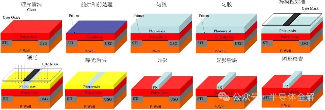
The surface of the substrate usually adsorbs H2O molecules from the air, which is detrimental to the lithography effect, so the substrate needs to be dehydrated first, which is the baking process.
For substrates with hydrophilic surfaces, the adhesion between them and the hydrophobic photoresist is insufficient, which can lead to issues such as photoresist peeling or pattern shifting. Therefore, a layer of adhesion promoter needs to be applied to the surface. Currently, commonly used adhesion promoters are hexamethyl disilazane (HMDS) and trimethylsilyl-diethyl-amine (TMSDEA).
Once the surface treatment is complete, we begin to spin coat the photoresist. The thickness of the photoresist after spin coating is related not only to the viscosity of the photoresist itself but also to the rotational speed used during spin coating. It can be roughly considered that the thickness of the photoresist is inversely proportional to the square root of the rotational speed. After spin coating, baking is required to evaporate the solvent from the photoresist, which further enhances its adhesion; this process is called pre-baking.
After all the above steps are ready, we move on to the exposure stage.
Photoresists can be positive or negative, and their properties after exposure are exactly opposite.
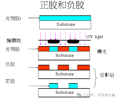
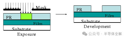
Taking positive resist as an example, unexposed photoresist is insoluble in the developer, while after exposure, it becomes soluble in the developer. During exposure, the light source illuminates the spin-coated substrate through a patterned mask, causing the photoresist to become patterned. Generally, before exposure, the substrate needs to be aligned with the mask to accurately control the exposure position. The exposure time must be strictly controlled; both too long and too short can lead to pattern distortion. After exposure, sometimes the substrate needs to be baked again to eliminate standing wave effects, but this step is not mandatory and can be skipped to go directly to development. The process of placing the substrate in the developer to dissolve the exposed photoresist is called development, with the aim of accurately copying the pattern from the mask onto the photoresist. The development time must also be strictly controlled; if too short, development will be incomplete, and if too long, pattern distortion will occur.
Next is hardening, where further baking makes the photoresist film adhere more firmly to the substrate surface and also increases the etch resistance of the film; the hardening temperature is generally slightly higher than that of the pre-bake temperature.
Finally, the pattern needs to be inspected under a microscope to see if it meets expectations. After transferring the pattern to the material through other processes, the photoresist completes its mission and needs to be removed. There are two methods for removing the photoresist: wet and dry. The former uses strong organic solvents (usually acetone) to dissolve the photoresist, while the latter uses oxygen plasma to etch away the photoresist.
Doping technology is also indispensable in semiconductor technology, as it can change the electrical properties of semiconductor materials as needed. Common doping methods generally include two types: thermal diffusion and ion implantation.
Ion implantation is a process that uses high-energy ions to bombard the semiconductor substrate directly for doping. Compared to thermal diffusion, ion implantation has many advantages. The ions to be implanted are screened using a mass analyzer, ensuring high doping purity. During the entire implantation process, the substrate is generally maintained at room temperature or slightly higher, and many masking films can be chosen, such as silicon dioxide (SiO2), silicon nitride (Si3N4), and photoresist, making the self-aligned masking technology very flexible. The dosage of ion implantation can be precisely controlled, and the distribution of impurity ions in the same plane after implantation is very uniform, with high repeatability of the implantation results.
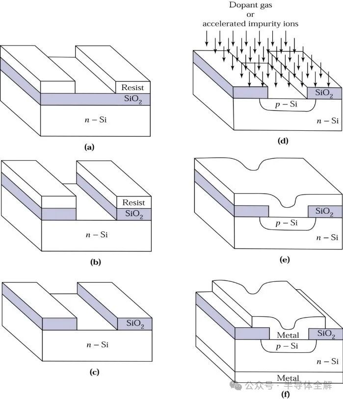
The depth of ion implantation is determined by the energy of the implanted ions. By controlling the energy and dosage of the ions, the distribution of impurity ions in the substrate can be manipulated, and different implantation schemes can be implemented multiple times to obtain various forms of impurity distribution. It is worth noting that in the case of a single crystal substrate, if the direction of ion implantation is parallel to the crystal orientation of the substrate, a channeling effect will occur, meaning that some ions will move along the channel, making the implantation depth difficult to control.
To avoid the channeling effect, the main axis direction of the single crystal substrate is typically tilted about 7° away from the implantation direction, or a layer of amorphous medium is covered on the surface of the substrate.
Although ion implantation has many advantages, it also has unavoidable disadvantages, such as significant damage to the crystal structure of the substrate. High-energy ions implanted into the substrate transfer energy to the substrate’s atomic nuclei and electrons through collisions, causing them to escape from the lattice and enter the gaps, forming interstitial-vacancy defect pairs. When the damage is severe, certain regions of the substrate’s crystal structure may be completely destroyed and become disordered amorphous areas.
Lattice damage greatly affects the electrical properties of semiconductor materials, such as reducing carrier mobility and decreasing the lifetime of non-equilibrium carriers. Most importantly, the implanted impurities are mostly located in irregular interstitial positions, making effective doping impossible. Therefore, it is essential to repair lattice damage and electrically activate impurities after ion implantation.
Thermal annealing is the most effective method for repairing lattice damage caused by ion implantation and electrically activating impurities. At high temperatures, interstitial-vacancy defect pairs in the substrate’s crystal will disappear due to recombination; amorphous areas will also begin to recrystallize from the interface with single crystal areas through solid-phase epitaxy. To prevent oxidation of the substrate material at high temperatures, the thermal annealing process must be conducted in a vacuum or inert gas environment. Traditional thermal annealing requires a long time, which can lead to severe impurity diffusion and redistribution.
The emergence of RTP technology solves this problem, allowing for significant repair of lattice damage and electrical activation of impurities while shortening annealing time.
According to different heat sources, RTP can be divided into several types: scanning electron beam, pulsed electron beam and ion beam, pulsed laser, continuous wave laser, and broadband incoherent light sources (halogen lamps, graphite heaters, arc lamps), among which broadband incoherent light sources are the most widely used. They can heat the substrate to the desired temperature in an instant and complete annealing in a short time, effectively reducing the degree of impurity diffusion.
PECVD is one of the methods of chemical vapor deposition (CVD) coating, along with atmospheric pressure CVD (APCVD) and low-pressure CVD (LPCVD).
Currently, PECVD is the most widely used among the three types, as it utilizes radio frequency (RF) plasma to initiate and maintain chemical changes, and this chemical change can occur in a non-high-temperature environment, resulting in low film deposition temperatures and high deposition rates, as shown in the schematic diagram of the equipment.
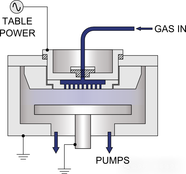
This method produces films with excellent adhesion and electrical properties, very low micropore density, high uniformity, and strong small-size filling capability. Factors affecting the quality of PECVD films include substrate temperature, gas flow rate, pressure, RF power, and frequency.
Sputtering is a physical vapor deposition (PVD) coating method. Charged ions [generally argon ions (Ar+)] are accelerated in an electric field and gain a certain amount of kinetic energy, which directs them toward the target material, colliding with target molecules to cause them to be ejected. These molecules also carry a certain amount of kinetic energy, moving toward the substrate and depositing on it.
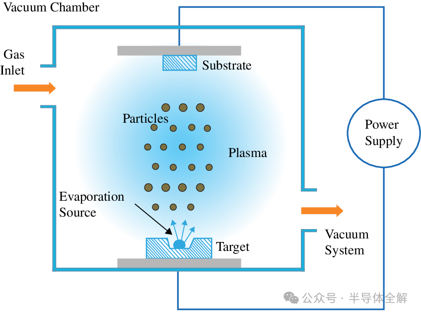
Common sputtering power supplies include DC and RF types; DC sputtering can be directly used for metals and other materials with good conductivity, while insulating materials can only be deposited using RF sputtering.
Ordinary sputtering has a low deposition rate, high working pressure, and poor film quality, while the emergence of magnetron sputtering ideally solves this issue. It uses an external magnetic field to change the ion’s motion trajectory from a straight line to a helical curve around the magnetic field direction, extending the ion’s motion path, enhancing the collision efficiency with target molecules, thus improving sputtering efficiency, increasing deposition rates, and lowering working pressure, greatly enhancing film quality.
Etching can be done using dry or wet methods; the former does not use a solution, while the latter uses specific solutions, hence the names of the two etching processes.
Generally, before etching, a masking layer needs to be prepared using lithography (which can be directly done with photoresist) to protect the areas that do not need to be etched.
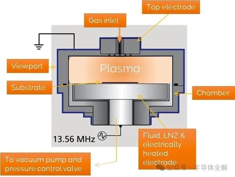
Common types of dry etching include inductively coupled plasma (ICP) etching, ion beam etching (IBE), and reactive ion etching (RIE).
In ICP etching, the plasma generated by glow discharge contains a large number of highly chemically reactive free radicals (free atoms, molecules, or atomic clusters), which react with the target material to produce volatile products, achieving the etching purpose.
IBE uses high-energy ions (from the ionization of inert gases) to directly bombard the target material’s surface to achieve etching; this is a physical process;
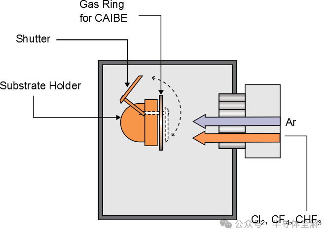
RIE can be seen as a combination of the previous two, replacing the inert gas used in IBE with the gas used in ICP etching, thus becoming RIE.
For dry etching, the vertical etching rate is much greater than the lateral etching rate, meaning a high aspect ratio, allowing for precise replication of the patterns on the masking layer. However, dry etching also has a certain etching effect on the masking layer, with poor selectivity (the ratio of etching rates for target materials and masking layers), especially for IBE, which may etch the material surface indiscriminately.
Wet etching refers to the method of achieving etching effects by placing the target material in a solution that can chemically react with it (i.e., etching solution).
This etching method is simple to operate, cost-effective, and has good selectivity, but has a low aspect ratio, and the materials protected under the masking layer’s edge may suffer corrosion, making it less precise than dry etching. To reduce the negative impact of low aspect ratios, suitable etching rates must be chosen.Factors affecting etching rates include etching solution concentration, etching time, and etching solution temperature.