Suddenly got stuck, what did I learn? Let me ask you, what is the maximum input conversion range of an ADC? (You can answer that in your mind, I can’t hear you), suddenly I was lost, what is it? This is the problem that this short article addresses.The ADC converts the input analog signal into a digital value by comparing it with a reference voltage.If the reference voltage is 3.3V, the typical input range of the ADC is 0~3.3V (unipolar) or -1.65V~+1.65V (bipolar, requiring a negative reference voltage). In other words, the value from the reference to ground potential is the range that can be processed.Furthermore, the resolution of our ADC (such as 12-bit, 16-bit) is based on the reference voltage. For example, the minimum resolvable voltage of a 12-bit ADC is VREF / 4096. This means that the final converted voltage is essentially how many parts of the resolvable voltage above it.Next, let’s look at some ADC reference ranges: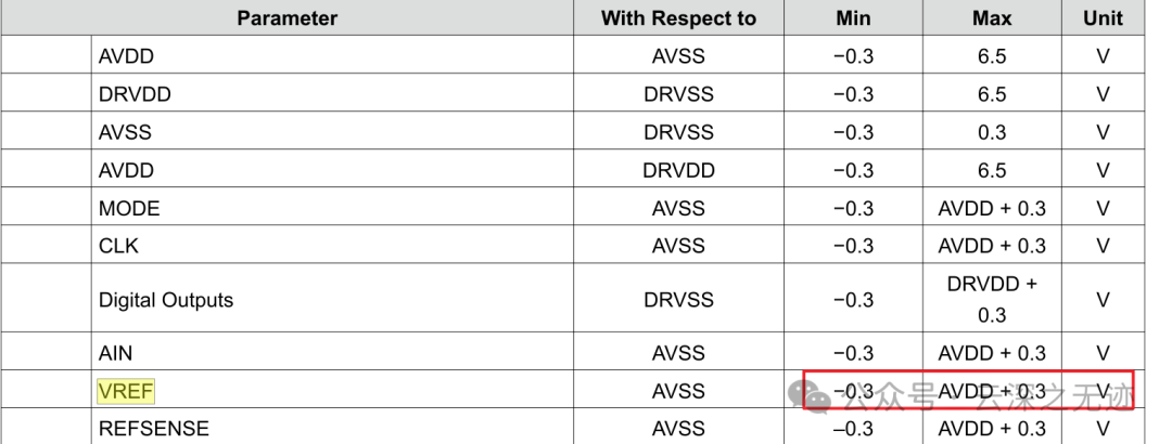 This is yesterday’s ADC, from 3PEAK.
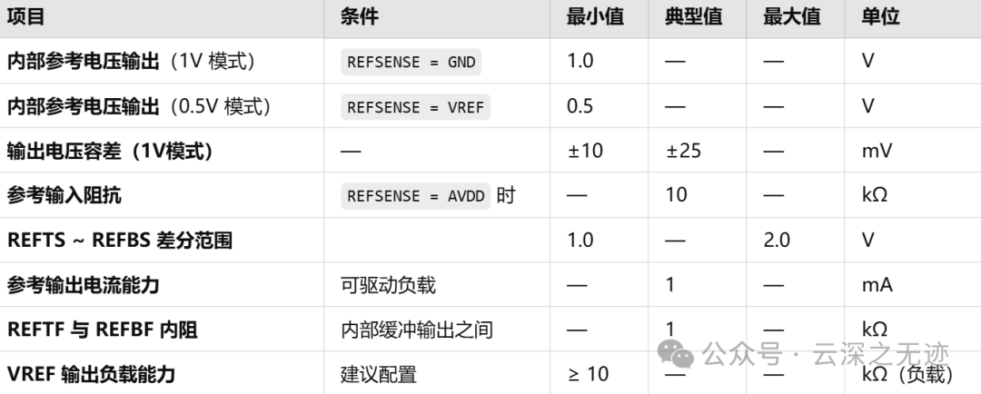 The provided parameters are quite comprehensive.
 It can’t be said that it’s completely incomprehensible; generally, our usage is quite rough.Let me also provide the role of the parameters:
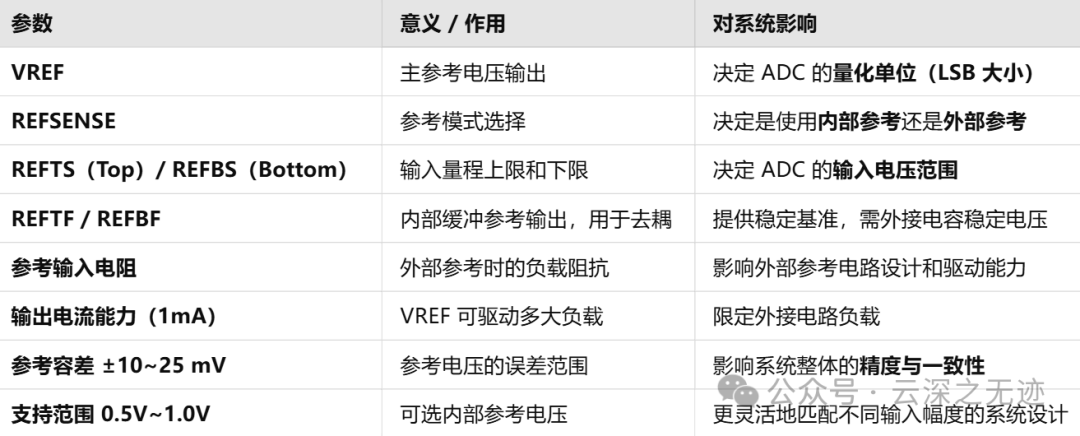 Alright, let’s pretend to understand.
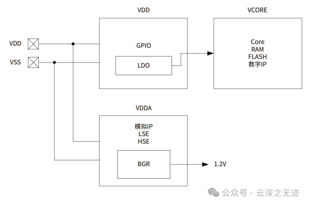 Our old acquaintance, CW32, references from the internal power supply.
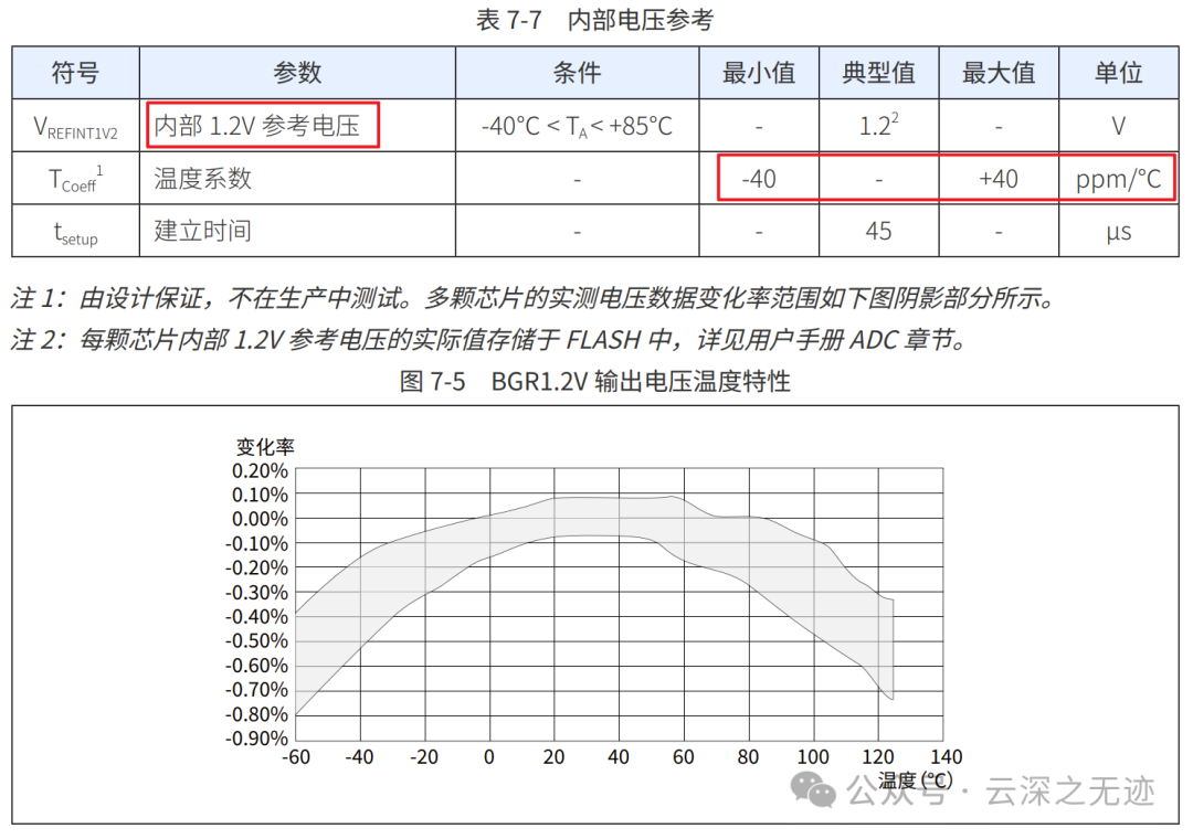 Only 1.2V, and it also shows a temperature-related relationship.Now let’s take a look at STM32:
 It is written like this:
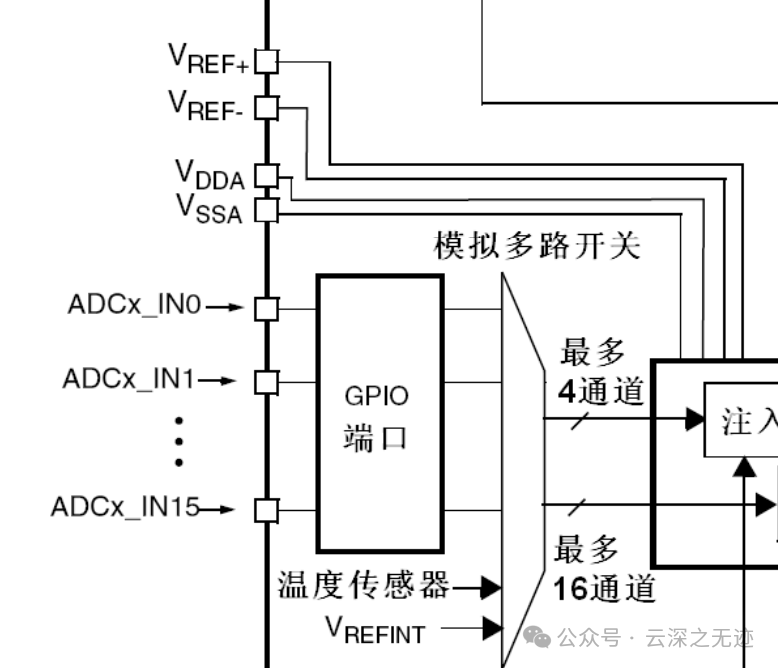 The block diagram is still quite understandable.
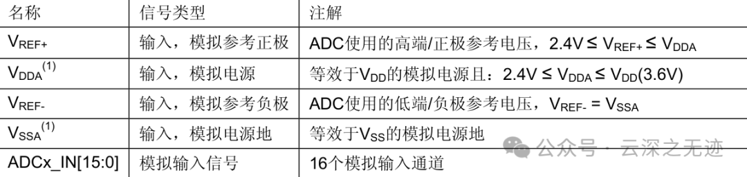 These two pins determine the measurement range of the ADC:
- ADC measurement range = VREF- (lower limit) ~ VREF+ (upper limit)
- Under normal circumstances: VREF- = VSSA (ground), VREF+ = VDDA (3.3V)
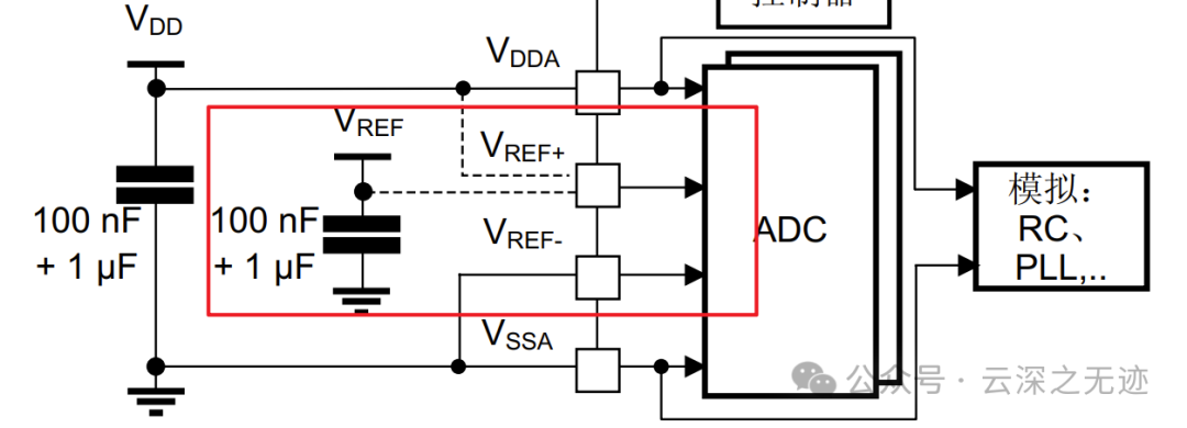 This is the internal reference of F4.
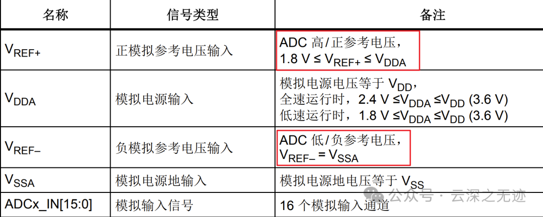 It must be greater than 1.8V, but below the supply voltage.
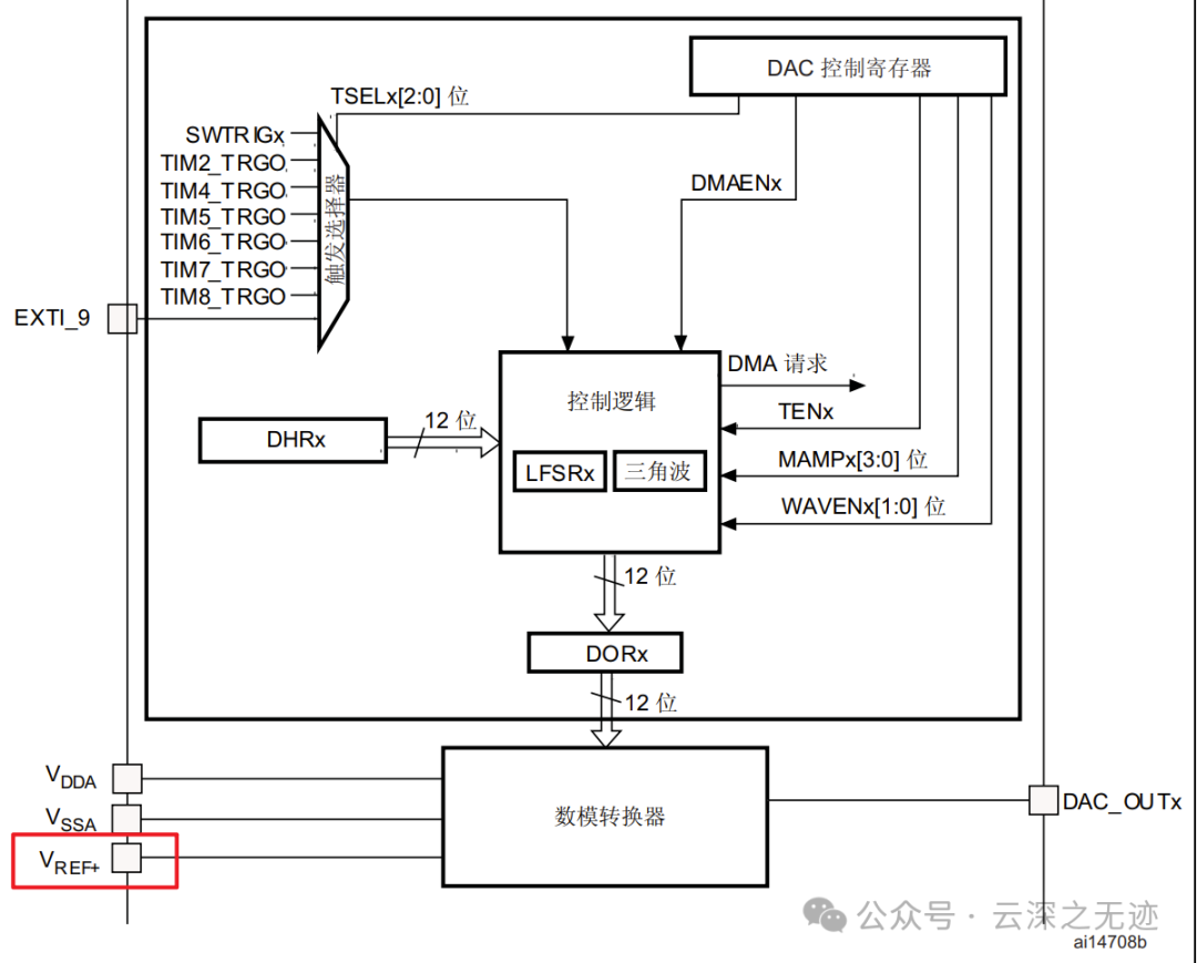 There is also a reference in the DAC.
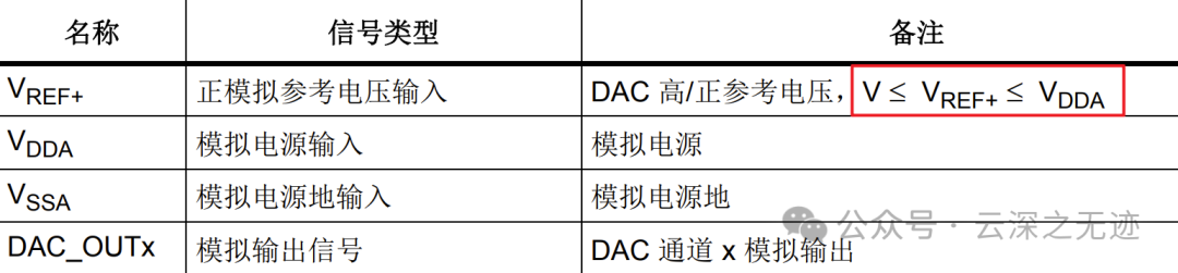 What is V? I don’t know.
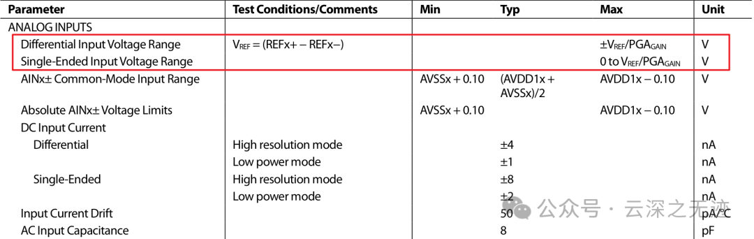 Now let’s look at the AD7771.
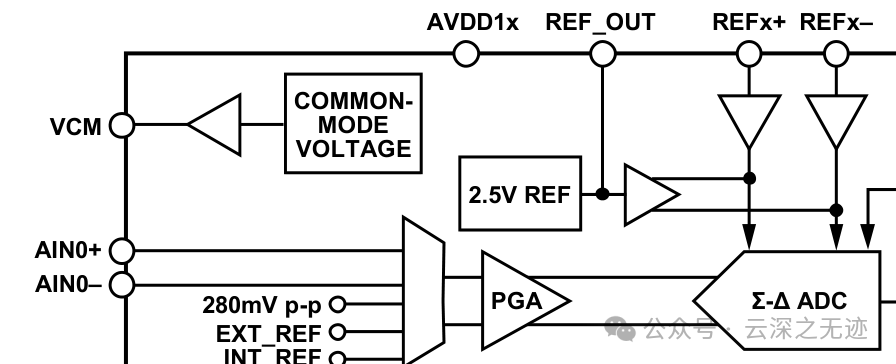 These ADCs have true differential inputs, so this reference is also dual.AD7771 is a true differential input architecture, and the analog input range is related to the reference voltage:
 When PGA ≠ 1, the input range is reduced, effectively increasing sensitivity:
 VREF = 2.5V, PGA = 4, full-scale input = ±0.625V.
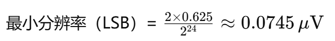 Very low, and also very delicate.Effective resolution can be derived from RMS Noise, assuming reference voltage VREF = 2.5V, PGA = 1, input range ±2.5V:
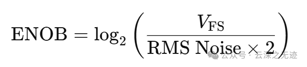 The multiplication by 2 is because the differential input has both positive and negative swings.
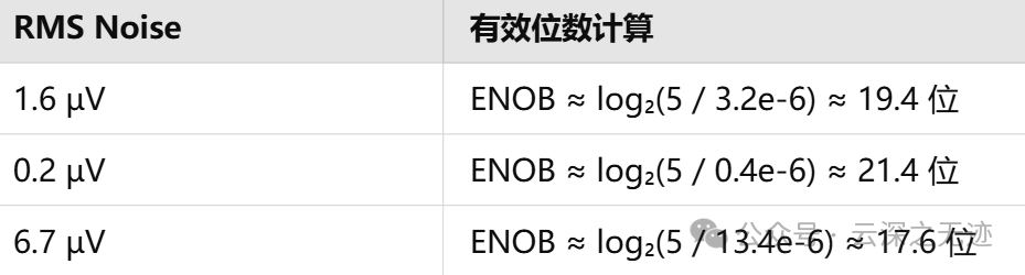 Calculation is complete.This learning is becoming more and more detailed.