Source: Semiconductor Industry Observation
No matter how elegant and clever the design of the computing engine is, the difficulty and cost of migrating existing (sometimes very old) code from currently running devices to new computing engines is a major barrier to adoption.
This is a particularly high barrier, as the inevitable unloading methods are still a novelty in the supercomputing field. In the early 21st century, with the support of the U.S. Department of Energy’s National Nuclear Security Administration, IBM developed the “Roadrunner” supercomputer at Los Alamos National Laboratory. Roadrunner was a pioneer in architecture, making Nvidia and other companies realize that they could also build unloading engines with powerful computing capabilities.
The architectural design of Roadrunner combined four IBM “Cell” PowerXCell floating-point vector engines with a pair of AMD Opteron X86 server CPUs, breaking the petaflop barrier in 2008 and laying the foundation for the future hybrid computing architectures familiar to today’s HPC and AI applications.
But no one said that programming these hybrid devices is easy, and Roadrunner was particularly difficult to program because it was the first of its kind. There were many complaints; it took some of the smartest people on Earth to get the machines to work. (Fortunately, Los Alamos has quite a few of the smartest people on Earth.) Nowadays, programming Nvidia GPUs is relatively easy because Nvidia has put immense effort into creating the CUDA programming environment and a plethora of libraries, frameworks, and algorithms.
Keep in mind: 75% of Nvidia’s employees work in software, even though most of its revenue (90%, 95%, or 99.5%) comes from hardware?
What if all this were unnecessary? What if you could just throw C++ or Fortran code at a massive data flow engine that could reconfigure itself for your code and do this automatically at runtime, continuously adjusting and readjusting itself as different code blocks are activated?
This is the dream of Elad Raz and the team he assembled at NextSilicon, which this week unveiled its second-generation Maverick-2 data flow engine, entering the HPC market with a new hardware and software approach.
It’s hard to believe, isn’t it? How many innovations and novel architectures have we heard about over the years with “magic compilers”? Too many to count. But like the HPC market itself, we still hope that with the right level of abstraction and appropriate automation, the work of executing code across different types of computing engines can become easier. Perhaps now is the time. Either do it or leave the work of porting code and creating new code to GenAI robots, because even if you pay them hundreds of thousands of dollars a year, there aren’t enough people in the world willing to do this extremely difficult task.
NextSilicon was founded in 2017, long before the GenAI craze, but at that time people were already aware that HPC and AI computing engine architectures would diverge, which is not favorable for the HPC simulation and modeling crowd focused on 64-bit and 32-bit floating-point computing. Even without initial plans to directly enter the AI market like Cerebras Systems, Graphcore, Groq, Habana Labs, Nervana Systems, and SambaNova Systems, NextSilicon has managed to raise $202.6 million in three rounds of funding, with its Series C round completed in June 2021, raising $120 million.
At that time, NextSilicon was valued at about $1.5 billion, and this funding and the completion of prototype work meant that the U.S. Department of Energy could understand NextSilicon’s trajectory. Sandia National Laboratory and NextSilicon collaborated to design and test the Maverick-1 data flow engine, and Sandia is currently building a new architecture supercomputer nicknamed “Spectra” as part of its Vanguard-II program. It is speculated that this will be built using the Maverick-2 data flow engine released today—Sandia has not disclosed this, nor does NextSilicon have the authority to do so. We expect Spectra to be installed in the first quarter of 2025, at which point there will be a more in-depth study of the Maverick-2 chip and the systems it uses.
What Raz can reveal is that the U.S. Department of Energy and the Department of Defense are collaborating with it, and many other organizations in the U.S. and Europe are also working with it.
Why Do We Need Another HPC Accelerator
The good news for global HPC centers is that Maverick-2 is targeting them, and NextSilicon will not be trying to chase the AI training and inference market for now.
“There are no accelerators specifically designed for high-performance computing,” Raz told The Next Platform. “We have hundreds of companies accelerating for AI and machine learning, and most large vendors are turning to AI machine learning. You can see what large supercomputers mean to them—they just need to build a new GPU cluster that costs twice as much, consumes twice as much power, and you get the same FP64 floating-point operations. NextSilicon is an HPC-first company.”
Raz added that in the long run, it makes sense for NextSilicon to create computing engines suitable for AI work, because if all predictions are correct, you cannot ignore the market that will drive more than half of system sales in the coming years. (This is the latest view from Gartner and the latest forecast from IDC, both of which are adaptations of our data.)
Currently, NextSilicon has not disclosed many details about the internal structure of the computing engine it has created, and this is intentional. The company wants people to first focus on the software problems it is solving, and then delve into the precise information and speed of the Maverick-2 data flow engine early next year.
“NextSilicon’s focus is on using software to accelerate your applications,” Raz explained. “At its core is a complex software algorithm that understands what is important in the code and accelerates it. In contrast, most CPUs and GPUs are groups of processor cores arranged in some form. They receive instructions and try to build complex pipelines and vector instruction sets, executing out of order to reduce latency. We think this is the wrong approach. A better approach is to apply the Pareto principle and look at how 20% of the code takes up 80% of the runtime. Why don’t we apply the 80/20 rule to computation and memory? Why can’t we automatically identify important computational kernels and try to focus only on them?”
The simple answer is that it’s difficult, but that’s the secret of the Maverick platform. Once the Maverick compiler and scheduler create a flow graph of the data and operations contained in the program, the data flow engine etched in transistors is its physical representation.
Raz then described the secret: “Applications start running on the host, and then we automatically identify the compute-intensive parts of the code. We stay in the intermediate representation of the computation graph. We don’t change the graph to instructions. You need to think of it as an instant compiler for hardware. We keep the graph of the program and place it on the data flow hardware. We get telemetry data from the hardware and do it recursively, so we are always optimizing computation and memory at runtime.”
Conceptually, this process is like converting C, C++, or Fortran programs running on a CPU host or GPU accelerator into the Maverick data flow engine. The first step is to identify the “possible flows” in the program graph that Raz spoke about:
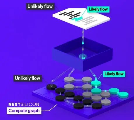
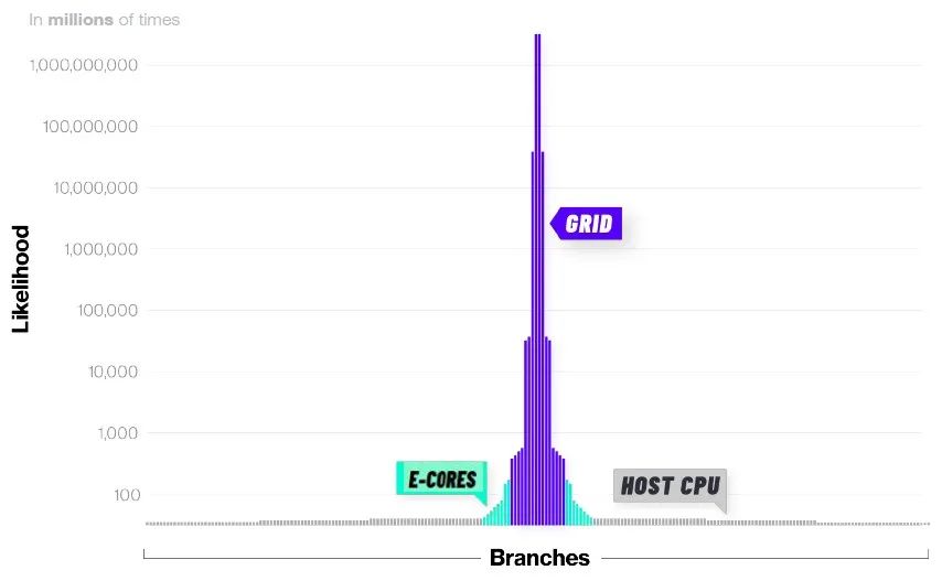
The possible and impossible flows in the code are projected onto the processing and memory element grid in the Maverick data flow engine, as shown below:
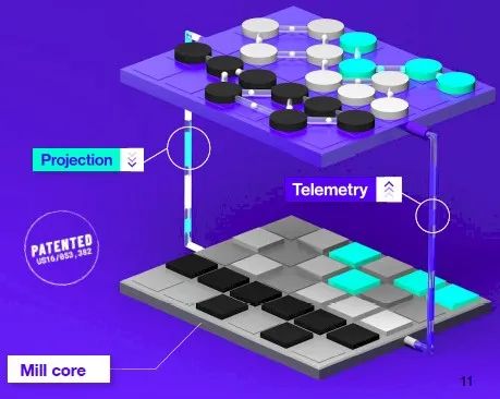
When the code runs on the data flow engine, performance bottlenecks in the first round of just-in-time compilation are identified, and telemetry data is sent back to the Maverick compiler to asymmetrically and iteratively rebalance the flow to create more “hardware” to support the possible flows and provide less “hardware” for the less likely flows. Certain types of serial work are offloaded to local and more traditional cores on the Maverick chip, while very heavy serial work is sent back to the host for faster execution. In this case, the host CPU is actually the serial engine offloading parallel Maverick data flow engine.
When the Maverick compiler has fully optimized the hardware configuration to run the possible and impossible flows, the system creates what is called a mill core:
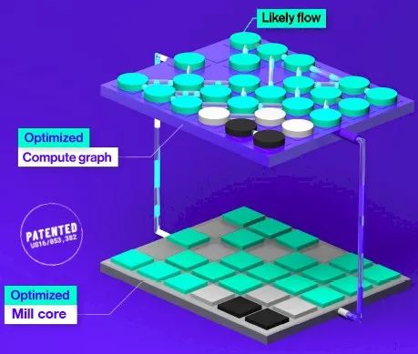
Given that application fragments are offloaded to the data flow engine, the mill core is designed to utilize as many resources in the data flow engine as possible; it is essentially a software-defined core created during operation to run the most likely parts of HPC code to accelerate them. The mill core is optimized for throughput rather than latency and emphasizes power efficiency over brute force. Importantly, the mill core can run hundreds or thousands of data flows in parallel, and they can replicate across data flow engines to work in parallel, just like real CPU cores and real GPU stream processors in physical devices. Therefore:
When you replicate hundreds to thousands of data flows across hundreds of mill cores, you achieve massive parallel processing, which can increase runtime by several orders of magnitude.
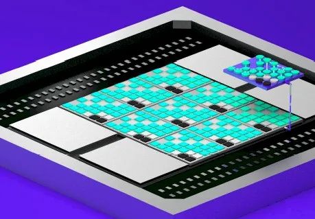
Another core idea is to put work and data onto the Maverick data flow engine and keep it there as much as possible to minimize data movement, which is a fatal issue in any hybrid architecture. If you do this, you will get a distribution of possible flows, reasonable flows, and impossible flows that looks like a futuristic skyscraper spanning three computing layers:
Beautiful, isn’t it?
This spider chart shows how the significant characteristics of the Maverick data flow engine compare to CPUs, GPUs, and FPGAs:
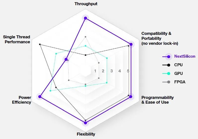
The goal is to achieve the flexibility, portability, and programmability of CPUs while providing better power efficiency and throughput than GPUs and FPGAs, sacrificing single-threaded performance that can be achieved through Maverick embedded cores (E cores) or host CPUs (which could now be Arm or X86 devices).
Currently, Raz has not disclosed what the E cores on the Maverick-2 chip are, but we can almost be certain that they are not Intel’s eponymous Atom heuristic E cores, and we are quite sure they are either licensed Arm cores or licensed or self-developed RISC-V cores. There are really no other practical options for 2024. (No one here is going to use IBM’s heavyweight Power cores.)
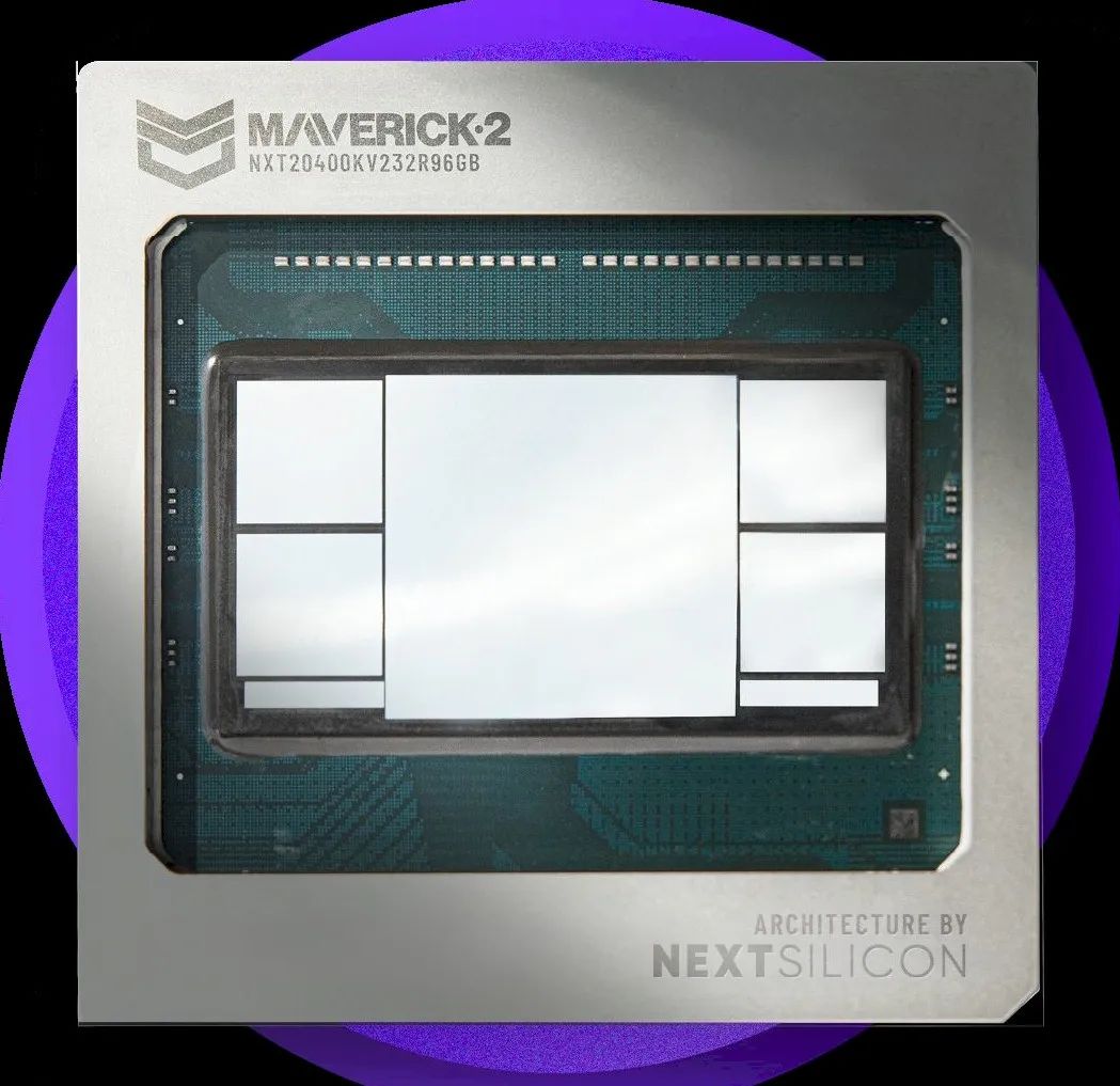
Now that we’ve first discussed software and have fundamentally changed the way we view the world, let’s finally take a look at the hardware of Maverick 2. This thing is a bit odd, but not crazy:
The Maverick-2 chip is etched using TSMC’s 5-nanometer process, and like many startups, hyperscalers, and cloud builders, it uses third-party designed chips, shipping computing engines to finished products through TSMC’s foundry and packaging partners. The chip has an area of 615 square millimeters, which, while not a die-shattering size, is not small either.
Overall, Maverick-2 has 32 E cores, and we see 256 computing elements—four elements per block, four blocks per row, and 16 rows per chip.
According to the specifications below, the device operates at a frequency of 1.5 GHz, and we assume that both the E cores and the data flow processing elements run at the same speed. (This may not be the case. You might want to run the E cores at a faster speed, such as 3 GHz, to handle serial work and lower it. If we designed the E cores on Maverick-2, they would have a base frequency of 1.5 GHz, accelerating to 3 GHz at runtime.)
From the specifications below and the packaging diagram above, the Maverick-2 chip has four sets of HBM memory, which in this case is HBM3E memory.
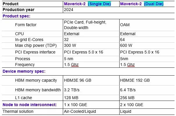
The dual-chip version of Maverick-2 supports the Open Compute Accelerator Module (OAM) form factor created by Microsoft and Meta Platforms to provide a universal accelerator slot for data center accelerators. Intel and AMD use OAM slots in their accelerators; Nvidia does not. The OAM version only publicly exposes a total of 16 PCI-Express 5.0 IO channels, rather than 32.
The thermal design point for each chip is 300 watts, so the specifications for the OAM unit are 600 watts, and only liquid-cooled versions are offered. This is the new standard for supercomputing, so no big deal.
Below is a conceptual diagram showing the two form factors:
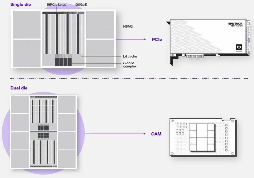
Don’t get hung up on the physical layout in the above image. We think it is not the same as the actual chip diagram shown above. You will notice that each Maverick-2 chip group has a 100 Gb/second RoCE Ethernet port for connecting accelerators together.
It is still unclear how the Maverick-2 devices will connect to shared memory clusters. We expect to learn more about this early next year.
Maverick-2 chips support C, C++, and Fortran applications using the OpenMP and Kokkos frameworks. Raz stated that NextSilicon will eventually support Nvidia CUDA and AMD HIP/ROCm environments as well as popular AI frameworks.
The peak theoretical performance of scalar, vector, and tensor units on the data flow engine will not be announced until the first quarter of 2025, and Raz does not place much importance on these numbers, as CPUs and GPUs have not yet reached their peak performance in this area.
“When you see many hardware vendors adding trillions of floating-point operations, peak performance isn’t important, but you can’t reach them because it only exists in GEMM, only in matrix multiplication, and only when you have local data,” Raz said. “The key to real applications is to use hardware more effectively, not to add a lot of floating-point operations that no one can reach.”
We ourselves can’t say it better. Given this, we wouldn’t be surprised to see the Maverick-2 chip reach hundreds of trillions of floating-point operations in vector and tensor FP64, and utilize them more fully on actual code than GPUs. In fact, this is the very premise on which NextSilicon was founded.
NextSilicon states in its background document that the performance per watt of Maverick-2 will be four times higher than that of Nvidia’s “Blackwell” B200 GPU. We know that the B200’s power consumption is between 1,000 and 1,200 watts, while a single Maverick-2 consumes 300 watts, and a pair of Maverick-2 in OAM packaging consumes 600 watts.
The document further notes that in various HPC simulations, the performance per watt of Maverick-2 is more than 20 times higher than that of the 32-core Intel “Sapphire Rapids” Xeon SP-8352Y Platinum processor, which has a rated speed of 18 trillion floating-point operations at FP64 precision, with a power consumption of 205 watts.
But as Raz points out, in this case, you not only need to test the strength of the Maverick compiler and its ability to create and replicate mill cores on the data flow engine, but also test the raw FP64 and FP32 performance of the chip. During benchmark runs, what we need to know is the total capability share of the device when running at a given rate, and then adjust based on cost.
We look forward to seeing the results from Sandia National Laboratory on the Spectra supercomputer. This could be very interesting, and we hope it can overturn many things. High-performance computing needs some love, not the floppiness of the AI crowd.
Reference Links
HPC Gets A Reconfigurable Dataflow Engine To Take On CPUs And GPUs