Old Chen is very pleased that many friends have recently added him on WeChat to express their gratitude, stating that they have benefited from his articles. Old Chen feels quite confused; as a newcomer to the screen industry, he encounters many specialized terms he does not understand; he sees many technical parameters he does not comprehend; he is unaware of industry rules; and he is unfamiliar with various business models. Whenever he does not understand something, he asks questions, often deep-seeking, frequently consulting experts and experienced peers from other fields. Old Chen enjoys expressing his questions in writing, but he often makes common knowledge errors, typos, and logical mistakes, and enthusiastic netizens frequently help correct him. Old Chen expresses his gratitude and hopes he has not misled anyone.This morning, I matched a 10.1-inch TFT screen for a client, with a size of 10.1 inches and parameters of 1280*800, using a MIPI interface. The main control chip is an Allwinner, with a MIPI 2 lane interface. The screen is for static data display, which has a low data volume. I chose the screen driver chip ILI9881C, which can operate in 2 Lane mode with LANSE = 1, perfectly matching the hardware and performance, with appropriate driver adjustments. To reduce system costs, a serial screen method using LT7589A RGB interface can be employed, which can save 30 yuan compared to the Allwinner chip. However, switching platforms is extremely difficult, and the only solution is to rely on standard screen suppliers, leading to an endless cycle of competition among screens.Not understanding is a reason to ask questions. Old Chen believes this article is very useful, so he decided to repost it, hoping to contribute to knowledge dissemination.
Introduction
MIPI (Mobile Industry Processor Interface) is an alliance established in 2003 by companies such as ARM, Nokia, ST, and TI, aimed at standardizing internal interfaces of electronic devices, such as camera, display, RF/baseband interfaces, etc., thereby reducing the complexity of electronic device design and increasing design flexibility. The benefit of a unified interface standard is that electronic device manufacturers can flexibly choose different chips and modules from the market according to their needs, making design and functionality changes quicker and more convenient.MIPI is not a single interface or protocol but includes a set of protocols and standards. The MIPI protocol mainly consists of three layers, from bottom to top: physical layer, protocol layer, and application layer.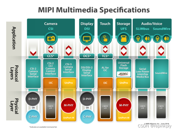
Hardware Introduction
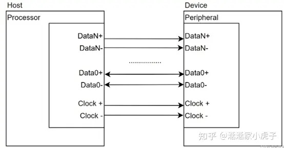
The hardware of MIPI refers to the physical layer, which currently includes four types: D-PHY, M-PHY, C-PHY, and A-PHY.D-PHY appeared in 2007.M-PHY was proposed in 2008. It has the highest data transmission capacity, but there are almost no practical application cases. The main reason is related to the development of camera applications; after reaching 20M pixels, cameras did not continue to develop significantly higher pixel counts as expected by the MIPI organization. Additionally, the development of M-PHY devices is overly complex, and without support from device manufacturers, D-PHY protocol remains in use.C-PHY protocol was proposed in 2013. Compared to M-PHY, it has a lower transmission speed but is more compatible with D-PHY and has lower device development costs.A-PHY v1.0 was proposed in September 2020, primarily addressing long-distance and reliability issues. It is expected to be mainly used in automotive scenarios in the future.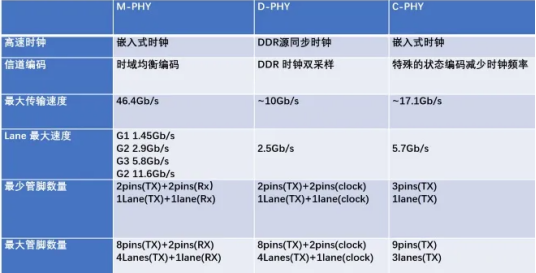 D-PHYThe D-PHY protocol supports a maximum of 5 lanes (one clock lane and four data lanes) and requires at least two lanes (one clock lane and one data lane). Each lane consists of two wires, P and N, with signals transmitted differentially, alternating between high and low in the same cycle. Data sampling occurs during both high and low clock signals. The clock lane is essential, while the number of data lanes can be selected based on the required data throughput.A lane represents a set of differential signals.D-PHY uses 1 lane of source-synchronous differential clock and 1/2/4 lanes of differential data lines for data transmission, making it a high-speed, low-power source-synchronous physical layer characterized by high speed, low power consumption, and low cost.The clock signal is unidirectional, provided from Master to Slave, and remains constant.The data signal can be unidirectional or half-duplex, meaning it can be transmitted in reverse. The essence of reverse transmission is actually reading data from the Slave by the Master. During reverse data transmission (Slave to Master), the bandwidth is only one-fourth of that during forward transmission (Master to Slave).D-PHY has many versions:
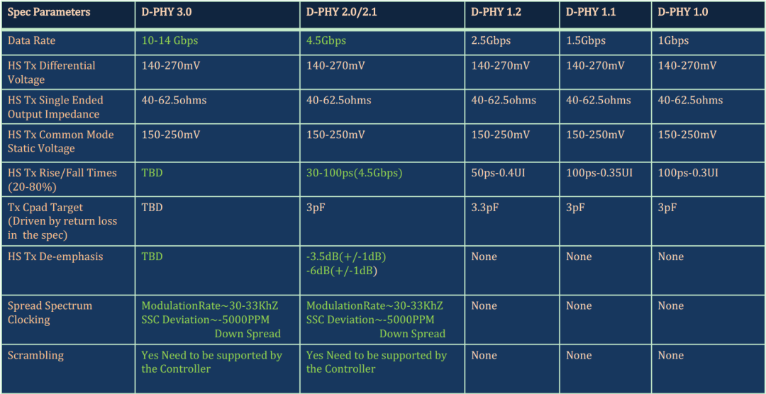 D-PHY Transmission StatesLow Power (LP) and High Speed (HS).LP (single signal 0V~1.2V): low power mode, 10Mbps transmission speed, asynchronous transmission, mainly used for transmitting control commands.HS (differential signal 100mv~300mv): high-speed mode, 80M~1Gbps transmission speed, synchronous transmission, used for transmitting high-speed image data.State Codes
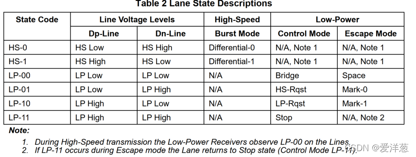 HS-0: Indicates that in High-Speed mode, the data on the Dp line is 0; since High-Speed is a differential signal, the Dn line is therefore 1.HS-1: Indicates that in High-Speed mode, the data on the Dp line is 1; since High-Speed is a differential signal, the Dn line is therefore 0.As mentioned earlier, in Low-Power mode, the two wires of a lane are independent and do not represent differential signals, so there are four possible expressions for the two wires:LP-00: Indicates that in Low-Power mode, the data on the Dp line is 0, and the data on the Dn line is 0.LP-01: Indicates that in Low-Power mode, the data on the Dp line is 0, and the data on the Dn line is 1.LP-10: Indicates that in Low-Power mode, the data on the Dp line is 1, and the data on the Dn line is 0.LP-11: Indicates that in Low-Power mode, the data on the Dp line is 1, and the data on the Dn line is 1.The Clock Lane generally uses a non-continuous clock signal mode. After transmitting a frame of image data, it switches back from HS mode to LP mode, and when the next frame of image data needs to be transmitted, it switches from LP mode to HS mode.D-PHY ModesControl Mode, Escape Mode, and High-Speed Mode (HS Mode). The first two modes belong to LP state, while High-Speed Mode belongs to HS state. Escape Mode is defined as a special operational mode under LP state.Burst Mode: High-Speed mode.Control Mode: Control mode under low power mode.Escape Mode: Escape mode under low power mode.During normal operation, the data channel is in High-Speed mode or Control mode.Burst Mode and Escape Mode cannot switch directly back and forth; they must go through Control Mode as an intermediary, i.e.: Burst Mode ↔ Control Mode ↔ Escape Mode.1. High-Speed Mode (Burst Mode)High-Speed mode is a mode under HS state used for image transmission. In High-Speed mode, the channel state is differential 0 or 1, meaning when the voltage on the Dp line is higher than that on the Dn line, it is defined as 1; when the Dp line is lower than the Dn line, it is defined as 0. The typical voltage on the line is a differential 200MV.2. Control ModeControl mode is a mode under LP state. The typical high level is 1.2V, and at this time, the signals on Dp and Dn are not differential signals but are independent of each other. When Dp is 1.2V and Dn is also 1.2V, the MIPI protocol defines the state as LP11; when Dp is 1.2V and Dn is 0V, it defines the state as LP10, and so on. In control mode, four different states can be formed: LP11, LP10, LP01, LP00.The MIPI protocol specifies that the four different states of control mode are composed in different sequences to represent entering or exiting a certain mode. For example, the sequence LP11-LP01-LP00 indicates entering High-Speed mode.3. Escape ModeEscape mode is a special operation of the data lane in LP state. In this mode, additional functions can be entered: LPDT (Low Power Data Transmission Mode), ULPS (Ultra-Low Power Mode), Trigger. Once entering Escape mode, the sender must send an 8-bit command to respond to the requested action.The data lane enters Escape mode through LP-11→LP-10→LP-00→LP-01→LP-00.To exit Escape mode: LP-10→LP-11.Under normal circumstances, the Data Lane is in High-Speed mode or Control mode. The timing for the Data Lane to enter Burst mode is shown in the following diagram:
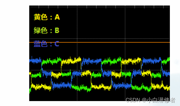
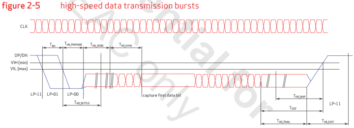 From this, it can be seen that the steps to enter HS mode from Control mode are LP11→LP01→LP00→HS0→SoT(00011101) → HS.Waveform DiagramThe yellow waveform of Channel 1 is P, and the blue waveform of Channel 2 is N, which clearly distinguishes the frame, line, and data intervals.Multiple frame intervals:
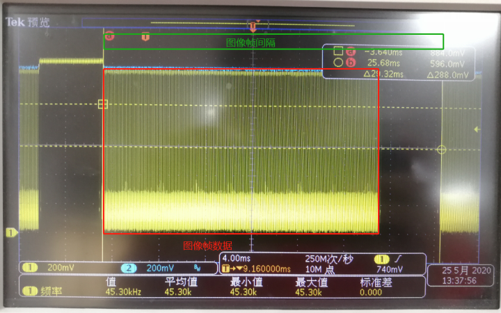
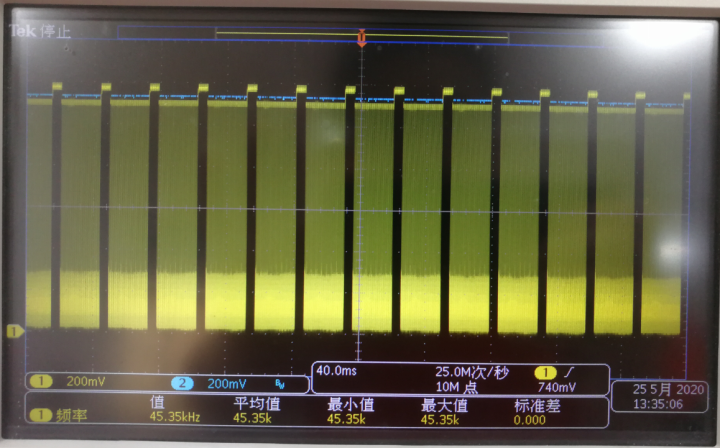 Image frame intervals (about 33 frames) and frame data:
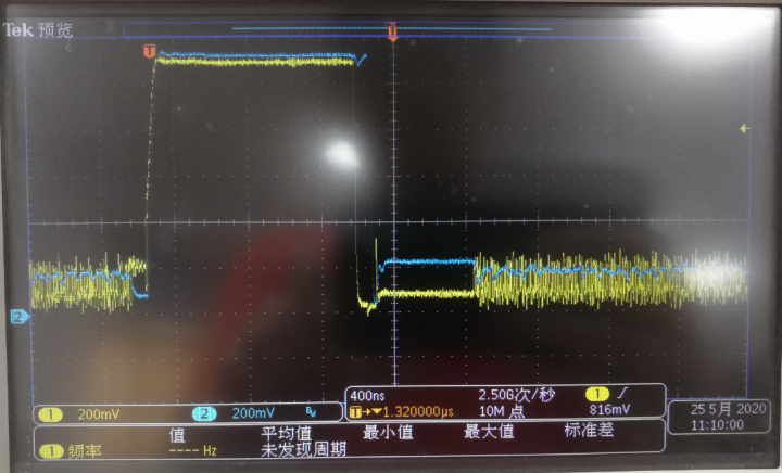
 LP transition process from HS to HS:
 Application Circuit
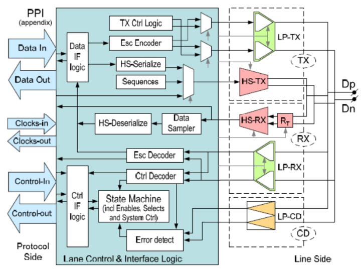
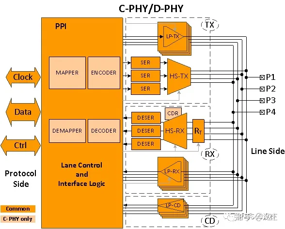
 Internal Structure
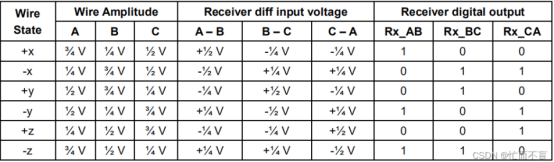
 C-PHYC-PHY is a three-wire system (A/B/C). It operates on three signals, integrating the clock into the data, thus eliminating the need for a separate clock channel.MIPI C-PHY requires CDR (Clock and Data Recovery); there is no direct transmission of CLK signals in the physical layer channel, and the clock frequency and phase need to be recovered from the received data.C-PHY and D-PHY can coexist on the same pins, allowing for compatibility.Wire StateThe C-PHY interface does not require a separate clock signal line but extracts it directly from the transmitted data. To effectively extract clock information from the data, the levels on the three signal lines A, B, and C must differ in the same cycle, resulting in six possible states based on their combinations.
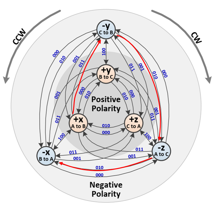
 For each state, there are five possible transitions to the next state.The information we need to transmit is encoded into the wire state. As mentioned earlier, C-PHY has six wire states: +x, -x, +y, -y, +z, -z. When the signal is in one of these states, it can only switch to one of the remaining five states; it cannot remain unchanged. Even if the data stream transmitted by C-PHY remains constant, the signal itself will continuously change. The information is encoded in the transitions between states, referred to as symbol encoding. In other words, there are only six paths; if you occupy one, you can only move to one of the remaining five paths. Thus, it is a base-5 system.Currently, we are using a base-5 system, with the maximum theoretical number of bits/symbol being log2(5) = 2.3219. The function of the mapper is designed to make the mapping rate as close as possible to but not exceed this theoretical limit. Additionally, the mapper must map between two integers. The choice of a ratio of 16/7 ≈ 2.28 is to achieve the above limitation.Another way to describe this is that the mapper needs to map 16 binary bits to a certain number of C-PHY symbols. But how do we determine how many symbols (S) to map to? There are 2^16 combinations on the parallel interface, and the combinations at the output of the mapper are 5^S => 2^16, so S = 7.
 Operating ModesLike D-PHY, C-PHY also has two operating modes: LP (Low Power) and HS (High Speed).
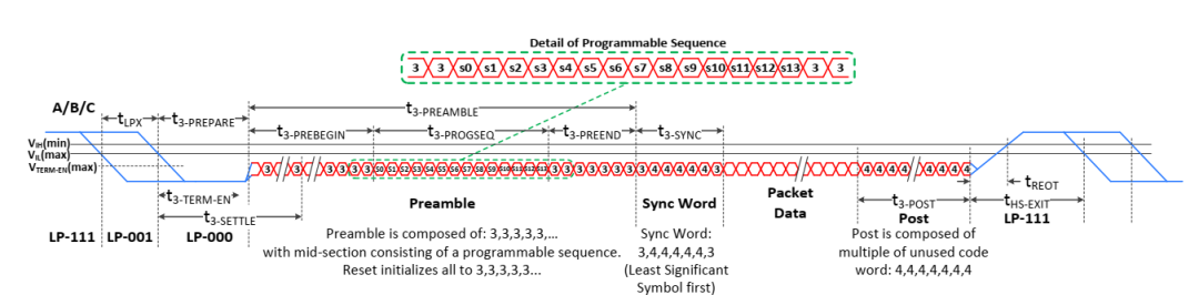 Waveform Diagram
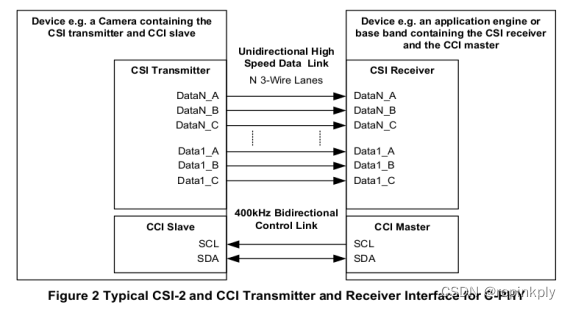
 Application Circuit
 C-PHY/D-PHY Combined IP
 A-PHYD-PHY, C-PHY, and M-PHY can handle large data volume physical transmissions, but these physical layer protocols cannot perform long-distance transmissions, leading to usage barriers in automotive and IoT fields. A-PHY is designed to provide data transmission physical layer support that can span the entire vehicle distance. Its maximum transmission distance can reach 15 meters, while the maximum transmission speed may reach or even exceed 48Gbps, far surpassing LVDS’s 1.5Gbps. It will help accelerate the performance of advanced driver-assistance systems (ADAS), autonomous driving systems (ADS), and automotive surround view systems, including cameras and in-vehicle infotainment (IVI) displays.The key technical advantages of A-PHY include:Asymmetric optimized architecture: A-PHY is designed from the ground up for high-speed asymmetric transmission from cameras/sensors to ECUs and from ECUs to displays, while providing concurrent low-speed bidirectional communication for command and control. Compared to other/symmetric architectures, the optimized asymmetric architecture simplifies design and reduces costs.Simplified system integration and cost reduction: Native support for devices using MIPI CSI-2 and DSI-2 ultimately eliminates the need for bridging ICs.Long-distance: 15-meter connection distance.High performance: 5-speed levels (2, 4, 8, and 16Gbps), with future speeds of 48Gbps or higher.End-to-end functional safety: A-PHY+CSI2/DSI2 can support functional safety from ASILB to ASILD.High reliability: Ultra-low error rate PER, 10^-19, can provide unprecedented performance throughout the vehicle’s lifespan.Mobile protocol reuse: After being successfully deployed in billions of smartphones and IoT devices, the MIPI protocol has been proven to be directly applicable to automotive use.Pure hardware protocol layer: Just like in mobile applications using D-PHY/C-PHY layering, A-PHY is tightly coupled with the CSI-2/DSI-2 protocol layer, essentially operating under a hardware-only protocol layer without software intervention. This architecture offers greater flexibility compared to other interfaces, which rely on software layers to achieve such flexibility.Optimized architecture for wiring, cost, and weight: Due to A-PHY’s optimized asymmetric architecture and hardware protocol layering, its implementation can meet optimized wiring, cost, and weight requirements. This becomes increasingly important as the number of electronic components and their interface cables increases on the path to autonomy.Flexible link layer support for other protocols: The MIPI Alliance aims to collaborate with other organizations applying their native protocols to automotive use. This includes VESA, which is adjusting its DisplayPort protocol specifications for automotive use. To accommodate these evolving specifications, A-PHY includes a universal data link layer that can accommodate different protocol adaptation layers and plans to support VESA’s automotive DisplayPort protocol.High EMC resistance: MIPI has invested heavily in analyzing and measuring harsh automotive channels and concluded that the architecture based on narrowband interference eliminators (NBIC) and unique PHY layer retransmission schemes (RTS) can provide the most robust performance, especially for applications requiring longer data rates.Currently, due to the lack of support for A-PHY in SoCs and devices, most scenarios require bridging chips for connection.
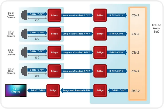 In the future, SoCs and devices with native support for integrated A-PHY will be able to connect directly.
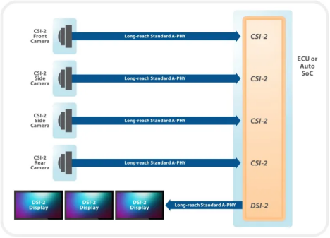 It can be seen that A-PHY is not a direct replacement for existing solutions but rather a compatible alternative to existing SerDes bridging chips, ultimately achieving a solution that does not require bridging chips. The benefit of this is a smooth transition, conducive to the acceptance and promotion of A-PHY.
Transmission Protocol
DSIMIPI DSI (Display Serial Interface) is a display interface technology developed by the MIPI Alliance, specifically designed to drive high-definition screens.The data transmission format of MIPI-DSI is based on packets, which are classified into short packets and long packets.Layered Architecture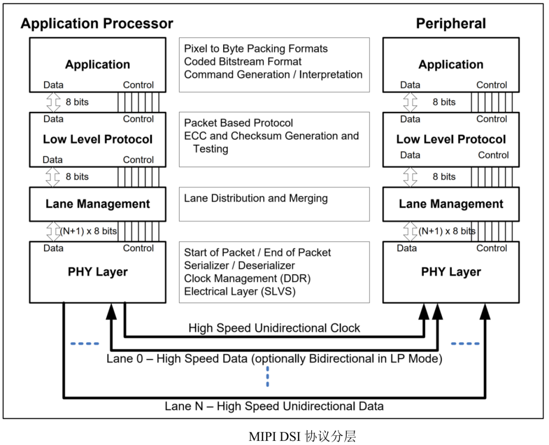 MIPI DSI consists of four layers, from top to bottom: application layer, protocol layer, link management layer, and physical layer.1. Application LayerThe application layer handles higher-level encoding, packaging the data to be displayed into the data stream, which the lower layers will process and send. The sender encodes commands and data in MIPI DSI format, while the receiver restores the received data to its original form.2. Protocol LayerThe protocol layer mainly packages data, adding ECC and checksums to the original data. The data passed down from the application layer is packaged into two formats: short packets and long packets. The sender packages the original data, adds headers and footers, and then sends the packaged data to the lower layer. The receiver performs the opposite operation upon receiving the data packet from the lower layer, removing the header and footer, and then using ECC to verify the received data. If there are no issues, the unpacked original data is handed over to the application layer.3. Link LayerThe link layer is responsible for how data is allocated to specific channels. MIPI DSI can support 1/2/3/4 lanes, depending on the actual application. If the bandwidth requirement is low, then 2 lanes are sufficient; if the bandwidth is high, then 4 lanes are needed. The data packets from the protocol layer are serial; if there is only 1 lane, then this 1 lane is used to send the data serially.4. Physical LayerThe physical layer is the lowest layer, completing the sending and receiving of MIPI DSI data on specific circuits. The physical layer is closely related to D-PHY and C-PHY. The physical layer specifies the entire electrical properties of MIPI DSI, such as voltage during signal transmission.Transmission ModesIn the link layer of MIPI DSI, there are two modes: video and command, which belong to the HOST side. Video and command are usually associated with HS and LP modes, but video and command belong to the Host category, while HS and LP belong to the D-PHY category.Data transmission in video mode has three timing modes:Non-Burst Mode with Sync Pulses: The peripheral can accurately reconstruct the original video timing, including the width of sync pulses.Non-Burst Mode with Sync Events: Similar to the above mode, but does not require precise reconstruction of sync pulse width, instead sending a “Sync event” packet.Burst Mode: In this mode, the time for sending RGB data packets is compressed, allowing for quick entry into LP mode after sending a line of data to save power.Short Packets4 bytes (fixed length) are mainly used for transmitting commands and reading/writing registers.Packet Header:· Data Identifier (DI) *1byte: Contains virtual data channel [7:6] and data type [5:0].· Data Packet *2 bytes: The data to be transmitted, fixed length of two bytes.· Error Correction Code (ECC) *1byte: Can correct a single bit error.Long Packets6~65541 bytes (dynamic length) are mainly used for transmitting large amounts of image data or partial control commands.Packet Header (4 bytes):· Data Identifier (DI) *1byte: Contains virtual data channel [7:6] and data type [5:0].· Word Count (WC) *2 bytes: The data to be transmitted, fixed length of two bytes.· Error Correction Code (ECC) *1byte: Can correct a single bit error.· Valid Transmission Data (6~65541 bytes): Maximum bytes = 2^16.· Packet Footer (2 bytes): Checksum.CSI-2CSI-2 (Camera Serial Interface 2) is an interface standard specified by the MIPI (Mobile Industry Processor Interface) Alliance’s Camera Working Group, primarily used to define the interface between camera peripherals and host controllers, aiming to establish standards for cameras and host controllers in mobile applications.In brief, CSI includes CSI-2 and CSI-3, with the main difference in implementation being the physical layer; CSI-3 requires M-PHY, while CSI-2 uses C-PHY and D-PHY, which will not be elaborated here.Layered Architecture
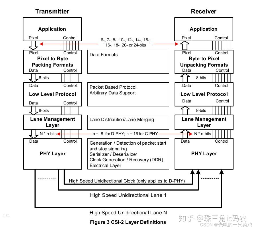 Application LayerPrimarily used for processing data in different scenarios. For the sender, it is mostly data generated by the camera; for the receiver, it is mostly SOC processing the data.Protocol LayerPixel Byte Conversion Layer: CSI-2 supports a variety of pixel formats. For the sender, before sending data, pixel data needs to be converted into the corresponding byte stream based on the pixel format; for the receiver, before providing data to the application layer, byte stream data needs to be converted back to pixel data.Low-Level Protocol Layer: Defines the byte stream protocol for packets between SoT and EoT, with the minimum unit of LLP being a byte.Lane Management Layer: Specifies that the number of lanes is expandable to meet bandwidth requirements in different scenarios.Physical Layer: The PHY layer specifies the transmission medium, capturing “0” and “1” from the serial bit stream while generating signals like SoT and EoT.D-PHY: D-PHY physically uses a 2-wire differential interface, consisting of one pair of differential clock lanes and one or more pairs of differential data lanes.GUI Tool: Introduction to LVGLJiangsu and Zhejiang still lack a “Beijing Diwen” serial screen module factory.Subscreen: Everything can be a screen.CarPlay vs Android Auto vs Car Life vs HiCar vs Carlink: An OverviewEntering the Factory Series: Hangzhou Vano
Old Chen has established a group chat for like-minded individuals to connect. The validity period is seven days; if it expires, please message Old Chen privately! Due to group chat size limitations, please add Old Chen on WeChat, and he will invite you to the main group.