(Written by Giacomo Paterniani, Field Application Engineer)
Abstract
This article demonstrates a method to accelerate the prototyping phase of embedded system design, illustrating how to combine hardware-independent drivers and sensors to simplify the device selection process for the entire embedded system. It will also introduce the components of embedded systems, typical software architecture, and the implementation of drivers. A follow-up article titled “Simplifying Embedded System Design with Hardware-Independent Methods: Driver Implementation” will further explore the execution process.
Introduction
By using hardware-independent drivers, designers can freely choose the type of microcontroller or processor to manage sensors without being constrained by hardware limitations. The advantage of this approach is that, in addition to the basic software layer provided by the vendor, additional software layers can be added while simplifying sensor integration. This article will use the Inertial Measurement Unit (IMU) sensor as an example to illustrate how to implement hardware-independent drivers; however, this method is also applicable to other types of sensors and devices. The drivers are written in C and tested on a general-purpose microcontroller.
Device Selection
The IMU sensor is primarily used for motion detection and measuring motion intensity through acceleration and angular velocity. In this example, the ADIS16500 IMU sensor is chosen (Figure 1) because it provides a simple and cost-effective method for precise multi-axis inertial detection and integration with industrial systems compared to complex and expensive discrete design solutions.
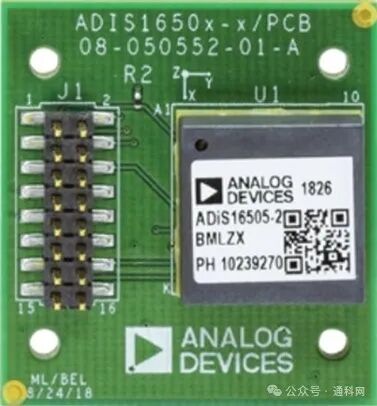
Figure 1. ADIS16500 Evaluation Board.
Main applications include:
* Navigation, stability, and instrumentation
* Drones and autonomous vehicles
* Smart agriculture and construction machinery
* Factory/industrial automation, robotics
* Virtual/augmented reality
* Motion IoT
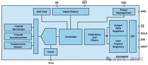
Figure 2. ADIS16500 Block Diagram.
The ADIS16500 is a precision micro-electromechanical systems (MEMS) IMU, featuring a three-axis gyroscope, a three-axis accelerometer, and a temperature sensor. See Figure 2. The sensitivity, bias, alignment, linear acceleration (gyroscope bias), and coordinate axis origin (accelerometer position) of this IMU have been factory calibrated. This means it can provide accurate sensor measurements under various conditions.
Through this interface, the microcontroller can write to and read from user control registers and read output data registers to obtain data from the accelerometer, gyroscope, or temperature sensor. All software and firmware required to manage this interface have been developed. Figure 2 shows the Data Ready (DR) pin. This pin is a digital signal indicating when new data can be read from the sensor. The DR pin can be treated as an input through a General Purpose Input/Output (GPIO) port, making it easy to manage via the microcontroller.
From a hardware perspective, the IMU sensor and microcontroller will be connected using an SPI interface, which consists of a 4-wire interface made up of nCS, SCLK, DIN, and DOUT pins. The DR pin should be connected to one of the GPIOs of the microcontroller. Additionally, the IMU sensor requires a power supply voltage of 3V to 3.6V, so 3.3V is sufficient.
Understanding the Typical Software Architecture of Embedded Systems
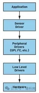
Figure 3. Software/Firmware Structure of Embedded Systems.
Understanding the general software and firmware structure of embedded systems is crucial for connecting to sensor drivers. This will help designers build a flexible software module that is easy to integrate into any project. Furthermore, drivers must be implemented in a modular way, allowing designers to rely on existing functions to add more advanced functions.
The software structure of embedded systems is shown in Figure 3. In Figure 3, the hierarchy starts from the application layer, where the application code is written. The application layer includes the main file, sensor-dependent application modules, and modules dependent on peripheral drivers that manage processor configurations. Additionally, all modules related to tasks that the microcontroller must handle are included in the application layer. For example, all software that manages tasks through interrupts or polling, state machines, etc. The application layer level varies depending on the type of project, so the code implemented in different projects also differs. In the application layer, all sensors in the system are initialized and configured according to their data sheets. All public functions provided by the sensor drivers can be called. For example, reading registers responsible for output data or writing to a register to change settings/calibration procedures.
Below the application layer is the driver layer for the sensors, which has two types of interfaces. All functions callable from the application layer are implemented at this layer. Additionally, the prototypes of the functions are inserted into the driver header file (.h). Therefore, by looking at the header file of the sensor driver, you can understand the driver interface and the functions that can be called from higher levels. The lower-level layers will connect with specific peripheral drivers that depend on the microcontroller managing the sensors. Peripheral drivers include all modules that manage the microcontroller peripherals, such as SPI, I2C, UART, USB, CAN, SPORT, etc., or modules that manage internal processor modules, such as timers, memory, ADC, etc. Because they are closely related to hardware, they are referred to as low-level functions. For example, each SPI driver is different due to the differences in microcontrollers. Taking the ADIS16500 as an example, the interface is SPI, so its driver will be encapsulated with the microcontroller’s SPI driver. The same applies to different sensors and different interfaces. For instance, if another sensor has an I2C interface, it will similarly be encapsulated with the microcontroller’s I2C driver during the sensor initialization process.
The lower layer of the sensor driver is the peripheral driver, which varies among different microcontrollers. As shown in Figure 3, the peripheral driver and low-level drivers are separate. Essentially, the peripheral driver provides read and write functions through available communication protocols. Since the low-level driver will manage the physical layer of the signals, it is highly dependent on the hardware used by the designer. Peripheral and low-level driver layers are often generated from the microcontroller’s integrated development environment (IDE) using visualization tools, depending on the evaluation board on which the microcontroller is installed.
Driver Implementation
The hardware-independent approach supports the use of the same driver across different applications, microcontrollers, or processors. This method depends on how the driver is implemented. To understand how the driver is implemented, we first look at the interface or the sensor header file in Figure 4 (adis16500.h).
The header file contains useful public macros. These include register addresses, maximum SPI speed, default output data rate (ODR), bit masks, and output sensitivities for the accelerometer, gyroscope, and temperature sensor, which relate to the number of bits (16 or 32) used to represent the data. Figure 4 shows these macros, with only a few register addresses displayed as examples.
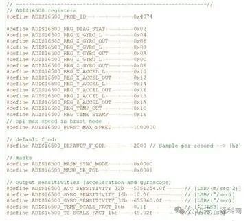
Figure 4. Macros displayed in the ADIS16500 header file (adis16500.h).
Figure 3 in the appendix shows all public variables and public type declarations available for each module, including adis16500.h, where new types are defined for more efficient data management. For example, the ADIS16500_XL_OUT type is defined as a structure containing three floats, one for each axis (x, y, and z). Additionally, enumerations are provided to support different sensor configurations, allowing designers to flexibly choose configurations that meet their needs. Notably, the part that makes the driver hardware-independent is at the beginning of the public variable section (Figure 3 in the appendix), where three key type definitions are present: pointers to three basic functions, or SPI send and receive functions, and a delay function required to generate the correct idle time between two SPI accesses. This code also shows the prototypes of the functions that can be pointed to. The SPI send function takes a pointer to the value to be sent as input and returns the content for checking to determine if the transmission was successful. The SPI receive function works similarly, taking a pointer to a variable as input, which will store the value read during reception. The delay function takes a float as input, representing the number of microseconds the designer wants to wait, and returns nothing (void). In this way, designers can use these specific prototypes in the application layer (e.g., in the main file) to declare these three functions. After declaration, they can assign these three functions to the fields of the ADIS16500_INIT private structure. An example is listed in Figure 2 of the appendix to help better understand the final step.
The SPI sender, receiver functions, and delay function are declared as static functions in the main file, thus belonging to the application layer. These functions depend on the peripheral driver functions, so the sensor driver itself is hardware-independent. These three functions are assigned to a variable’s fields, which are pointers to functions. This way, designers can encapsulate the sensor and microcontroller without modifying the sensor driver code. If designers change the microcontroller, they only need to replace the low-level functions within the three static functions with the corresponding functions of the new microcontroller, thus adjusting the main file. Through this method, the driver becomes hardware-independent because designers do not need to change the sensor driver code. The IDE of the microcontroller typically includes low-level functions such as spiSelect, spiReceive, spiUnselect, chThdSleepMicroseconds, etc. In this case, the microcontroller evaluation board used is the SDP-K1, which embeds the STM32F469NIH6 Cortex®-M4 microcontroller. The IDE is ChibiOS, a free Arm® development environment.
Figure 4 in the appendix shows the callable function prototypes at the application level. These prototypes, along with all other software and firmware discussed in Figures 2 and 3 of the appendix, can be found in the sensor driver header file (adis16500.h). First, the initialization function (adis16500_init) takes a pointer to the ADIS16500_INIT structure as input and returns a status code indicating whether the initialization was successful. The implementation of the initialization function is completed in the source file of the sensor driver (adis16500.c). Figure 5 in the appendix shows the code for the adis16500_init function. First, a type named ADIS16500_PRIV is defined, which contains all fields of the ADIS16500_INIT structure, and then a private variable _adis16500_priv of that type is declared. In the initialization function, all fields of the ADIS16500_INIT structure passed from the application layer will be assigned to the fields of the private variable _adis16500_priv. This means that any subsequent calls to the sensor driver will use the SPI read/write functions and processor delay functions passed in from the application layer. This is crucial because it allows the sensor driver to be hardware-independent. If designers want to change the microcontroller, they only need to change the functions passed to the adis16500_init function without modifying the sensor driver code itself. At the beginning of the initialization function, the initialized field of the _adis16500_priv variable is set to false because the initialization process has not yet been completed. At the end of the function, this field will be set to true, and then it will return. Every time a public function (Figure 4 in the appendix) is called, the following check is performed: if _adis16500_priv.initialized is true, it can proceed; if false, it will immediately return an ADIS16500_RET_VAL ERROR error. This is to prevent users from calling functions without first initializing the sensor driver. Continuing the discussion of the initialization function, the following steps are executed:
1. Check the pre-known product ID by reading the ADIS16500_REG_PROD_ID register.
2. Write the value passed from the application layer (main.c) to the corresponding bit field of the ADIS16500_REG_MSC_CTRL register to set the Data Ready (DR) pin polarity.
3. Write the value passed from the application layer (main.c) to the corresponding bit field of the ADIS16500_REG_MSC_CTRL register to set the synchronization mode.
4. Write the value passed from the application layer (main.c) to the ADIS16500_REG_DEC_RATE register to set the decimation rate.
The initialization function depends on the read/write register functions (Figure 6 in the appendix). Therefore, after assigning values to the _adis16500_priv variable, the above four routines need to be completed. Otherwise, when calling the read or write register functions, they will not know which SPI sender, receiver, and processor delay functions to use.
Referring to Figure 4 in the appendix, after the initialization function, other public functions can also be called. Below is a description of the functionality of the implemented routines, shown as low-level routines. The second part of this article will detail other implemented functions of the driver. All of the following functions can only be called after the initialization function. To this end, a careful check will be performed at the beginning of each function to determine whether the sensor has been initialized. If not initialized, the program will immediately return an error.
* adis16500_rd_reg_16
This function is used to read a 16-bit register. The implementation of this function can be seen in Figure 6 in the appendix. Inputs include ad, a uint8_t variable representing the address of the register to be read, and *p_reg_val, a pointer to a uint16_t type variable indicating the target where the read value will be assigned. To read the register via the SPI protocol, two SPI accesses are required; the first access is to send the address, and the second access is to read back the value of the addressed register. There needs to be an idle time between the two accesses, so a delay function is required. During the first access, we send the read/write bit, which in this case is 1 (R = 1, W = 0), the register address shifted 8 bits, followed by 8 bits of 0, so the sequence is as follows:
R/W | AD6 | AD5 | AD4 | AD3 | AD2 | AD1 | AD0 | 0 | 0 | 0 | 0 | 0 | 0 | 0 | 0 |
Where AD represents the address, and R/W represents the read/write bit.
After the delay, the function reads the value via SPI and passes that value to the input pointer. The registers of the ADIS16500 have a high address containing the high bits (8 most significant bits) and a low address containing the low bits (8 least significant bits). To obtain the complete 16-bit value (low and high), using the low address as ad is sufficient because the low and high addresses are contiguous.
* adis16500_wr_reg_16
This function is used to write to a 16-bit register. The implementation of this function can be seen in Figure 6 in the appendix. Inputs include ad, a uint8_t type variable representing the address of the register to be written, and reg_val, a uint16_t type variable representing the value to be written to the register. For the read function, both low and high addresses and low and high values need to be considered. Therefore, according to the data sheet, to write to the ADIS16500 registers, two SPI accesses are required during transmission. The first access will send a R/W bit equal to 0, followed by the low register address and the low value, so the sequence is as follows:
R/W | AD6 | AD5 | AD4 | AD3 | AD2 | AD1 | AD0 | D7 | D6 | D5 | D4 | D3 | D2 | D1 | D0 | where D represents data.
The second SPI access will send a R/W bit equal to 0, followed by the high register address and the high value, so the sequence is as follows:
R/W | AD14 | AD13 | AD12 | AD11 | AD10 | AD9 | AD8 | D15 | D14 | D13 | D12 | D11 | D10 | D9 | D8 |.
The write and read register functions can actually be defined as private, making them invisible and uncallable from outside the driver software module. They are defined as public to allow for debugging. This way, designers can quickly access any register in the sensor for reading or writing, helping to troubleshoot.
* adis16500_rd_acc
This function reads the x, y, z acceleration data from the output data register and returns their values in [m/sec²]. The implementation of this function can be seen in Figure 7 in the appendix. The input is a pointer to the ADIS16500_XL_OUT structure, which contains three fields represented as floats for x, y, and z acceleration. The method of reading acceleration is the same across all three axes, with the only difference being the register to be read. Each axis has its respective register to read: the x-axis must read from the x acceleration output data register, and the y and z axes read from their respective registers. The acceleration values will be represented as 32-bit values, so two registers need to be read. One reads the high 16 bits, and the other reads the low 16 bits. Therefore, as seen in the code, two register read accesses will be performed, along with appropriate shifting and OR operations to obtain the complete binary value, which will be stored in a private int32_t variable named _temp. The data will then be converted from binary to two’s complement. After conversion, the two’s complement value will be divided by the sensitivity (in [LSB/(m/sec²)]) to obtain the final acceleration value in [m/sec²]. This value will be recorded in the x, y, or z field of the pointer that points to the structure passed as input.
* adis16500_rd_gyro
The gyroscope read function is implemented in the same way as the acceleration read function. This function will read the x, y, z gyroscope data, with units in [°/sec]. Its implementation can be seen in Figure 8 in the appendix. Similar to the acceleration function, the input is a pointer to the ADIS16500_GYRO_OUT structure, which contains x, y, and z gyroscope data represented as floats. The registers read are the gyroscope output data registers. The binary values will be represented as 32 bits, and to obtain the two’s complement value, the same steps as in the acceleration function need to be completed. After converting from binary to two’s complement, the obtained value will be divided by the sensitivity (in [LSB/(°/sec)]) to finally yield a value in [°/sec], which will then be recorded in the x, y, or z field of the pointer that points to the structure passed as input.
Conclusion
This article outlines the typical software/firmware stack of embedded systems and introduces the driver implementation for IMU sensors. The hardware-independent approach provides a reusable method for various sensors or devices, regardless of the interface (SPI, I2C, UART, etc.). A follow-up article titled “Simplifying Embedded System Design with Hardware-Independent Methods: Driver Implementation” will further explain the implementation methods of sensor drivers.
Author Biography
Giacomo Paterniani holds a degree in Biomedical Engineering from the University of Bologna and a Master’s degree in Electronic Engineering from the University of Modena-Reggio Emilia. After graduation, he worked as a researcher at the University of Modena-Reggio Emilia for a year. In April 2022, he joined ADI’s graduate program as a Field Application Engineer. In April 2023, he became a Field Application Engineer.