This article is reprinted from the Jishu Community
Jishu Column: Agile MM32 MCU
Table of Contents
The previous article introduced the MM32F5 series which utilizes the “Star” STAR-MC1 processor. If readers recall, the “Star” processor has a significant advantage over the M3 and M4 processors by introducing a memory subsystem, including L1 instruction and data cache interfaces and a tightly-coupled TCM interface. However, having only the memory subsystem is not enough; it needs to be paired with an efficient bus architecture design to maximize its functionality.
This time, the author will discuss the bus architecture design of the MM32F5270 and see how the F5270 achieves maximum system throughput through high parallelism in bus design.
Bus Architecture of MM32F5270
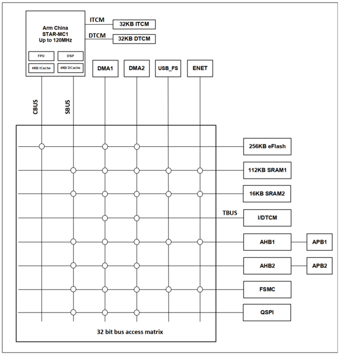
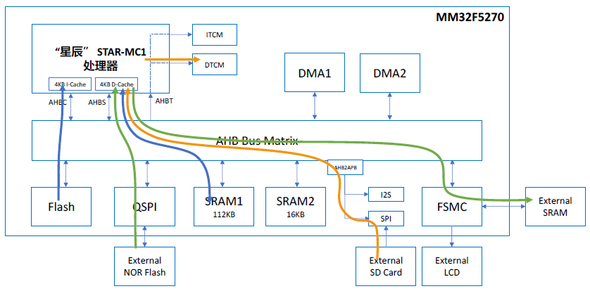
The diagram below illustrates the bus architecture of the MM32F5270. As can be seen, the processor, memory, and peripherals in the system are interconnected through a zero-latency AHB bus matrix. This bus matrix is a multi-master to multi-slave multi-layer AHB bus structure. Here, the party that can initiate read/write access is called the Master, while the responding party is called the Slave.
Note: AHB is a type of Arm® AMBA® communication interface protocol, which is one of the commonly used interface protocols in embedded systems. For readers unfamiliar with the Arm® AMBA® interface protocol, please refer to relevant materials; this article will not elaborate further.
Bus Master – Access Initiator
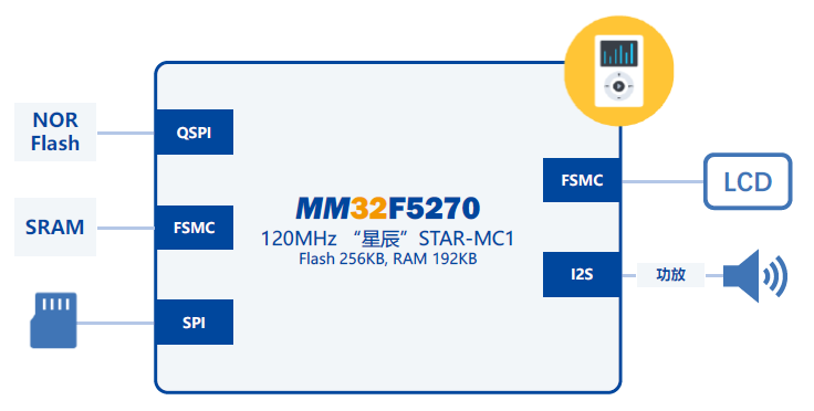
From the above diagram, it can be seen that the MM32F5270 includes the following AHB bus Masters:
Among them, the “Star” processor occupies three AHB ports: the system bus AHBS (system bus), the code bus AHBC (code bus), and the TCM bus AHBT (TCM bus). AHBC and AHBS are the paths through which the processor initiates access to obtain data and instructions from the outside, while AHBT is the path for other Masters outside the processor (like DMA) to access the internal TCM. This means that TCM can not only be accessed by the CPU but can also be accessed by external resources as ordinary SRAM.
Other Masters include DMA, USB, and Ethernet. In the MM32F5270, to improve system parallelism, two independent DMA controllers are configured, each containing 8 channels. Each DMA can perform read/write access to the Slave without CPU intervention. USB and Ethernet can also act as bus Masters to directly initiate access to system storage, for instance, moving data placed in SRAM to the TX FIFO for data communication without CPU intervention.
Bus Slave – Access Responder
The MM32F5270 includes the following AHB bus Slaves:
-
256KB Built-in Flash Memory
-
112KB SRAM1
-
16KB SRAM2
-
QSPI – Expandable Four-Line NOR Flash
-
FSMC – 8/16/32-bit Parallel Interface, Expandable SRAM, NOR Flash, 8080/6800 Display
-
Peripheral APB1 Group
-
Peripheral APB2 Group
-
32KB ITCM and 32KB DTCM – accessed via AHBT bus
To enhance system parallelism, the MM32F5270 is equipped with two independent RAMs: 112KB of SRAM1 and 16KB of SRAM2, each with its own RAM controller and Slave port.
Additionally, the MM32F5270 is equipped with 32KB of Instruction TCM RAM (ITCM) and 32KB of Data TCM RAM (DTCM). Here, TCM and CPU are directly connected through the TCM interface, which is equivalent to a fast lane. The CPU can access TCM without going through the external bus matrix, which is why TCM is referred to as Tightly-Coupled Memory (TCM). Accessing TCM by the CPU incurs no latency, so it does not require caching. At the same time, the “Star” processor also reserves the AHBT bus for access to TCM by external Masters like DMA. The AHBT bus is connected at the Slave end of the bus matrix, which means that DMA must go through the bus matrix to access TCM. When both DMA and CPU access TCM simultaneously, the “Star” processor gives priority to CPU access for arbitration. It should be noted that ITCM supports program execution and data reading, starting at address 0x0000_0000, while DTCM supports data reading starting at address 0x2000_0000.
Based on the above description, it can be concluded that the MM32F5270 is configured with 4 completely independent RAMs, including ITCM, DTCM, SRAM1, and SRAM2. In certain application scenarios, these 4 RAMs can be accessed simultaneously by different Masters without causing any bus conflicts or waiting. For example, the CPU can read and execute algorithms stored in ITCM, Ethernet can read and write data from SRAM2, DMA1 can transfer data from DTCM, and DMA2 can transfer data from SRAM1. These four paths are completely independent and parallel.
The MM32F5270 also includes two independent APB peripheral groups, namely APB1 and APB2, each with its own Slave ports and AHB to APB protocol conversion bridges.
Meanwhile, users can expand the system with FSMC to add parallel NOR Flash or SRAM, or use QSPI to expand four-line NOR Flash. Both FSMC and QSPI are directly connected to the zero-latency AHB bus matrix as AHB Slaves, so their access paths are completely independent. Of course, users can also expand more storage space through serial bus interfaces like SPI and UART, but these peripherals are connected to the APB bus, sharing the AHB Slave port of the bus matrix with other peripherals connected to the APB bus, which may result in additional wait cycles.
It should be noted that, apart from TCM and peripheral space, instructions and data read from the Code bus and System bus can generally be accelerated by the 4KB instruction cache and 4KB data cache.
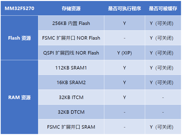
The following table summarizes the Flash and RAM resources supported by the MM32F5270:
Concurrent Network
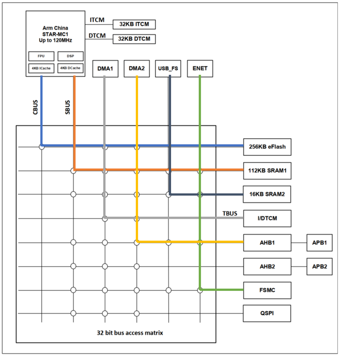
The connection relationship between Masters and Slaves in the aforementioned bus structure diagram is represented by hollow circles on the matrix network. For example, the built-in Flash can only be accessed by the CPU’s code bus or DMA, but not by other bus Masters.
The effect that can be achieved based on the above description is that multiple Masters can simultaneously initiate access to multiple Slaves. If the initiators (Masters) and responders (Slaves) of each path are different, then these accesses are completely parallel and do not require arbitration or wait cycles.
The following diagram is an example of concurrent access, where 6 bus Masters access 6 bus Slaves, forming 6 independent paths. Of course, this is just an extreme case. The actual concurrent effect achievable in a real application needs to be analyzed based on application requirements.
Case Study: Audio Player with Display
To illustrate the power of the F5270’s multi-concurrent bus design more intuitively, a practical application case is presented here. It should be noted that this case is only for explaining functionality and is not intended as a reference design.
Here, we consider creating an audio player with a display based on the MM32F5270. This is a common application scenario, and the actual product may include various functions. For simplification, we take the following specifications as an example:
-
Can play audio files on the SD card, supporting WAV and MP3 formats
-
2.4-inch screen, 320×240 resolution, GUI interaction
Note: Actual products may have more functions, such as higher resolution displays, USB expansion, WIFI or Bluetooth connectivity, video playback, touch control, etc. Interested readers can search for relevant products online.
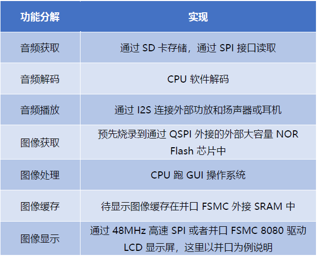
Based on these requirements, a display-equipped audio player can be built. According to the internal resources included in the MM32F5270, the following functional decomposition and resource allocation can be made for the above specifications:
The corresponding simplified system block diagram is as follows:
Analysis shows that the main functionality of the system can be divided into three parts:
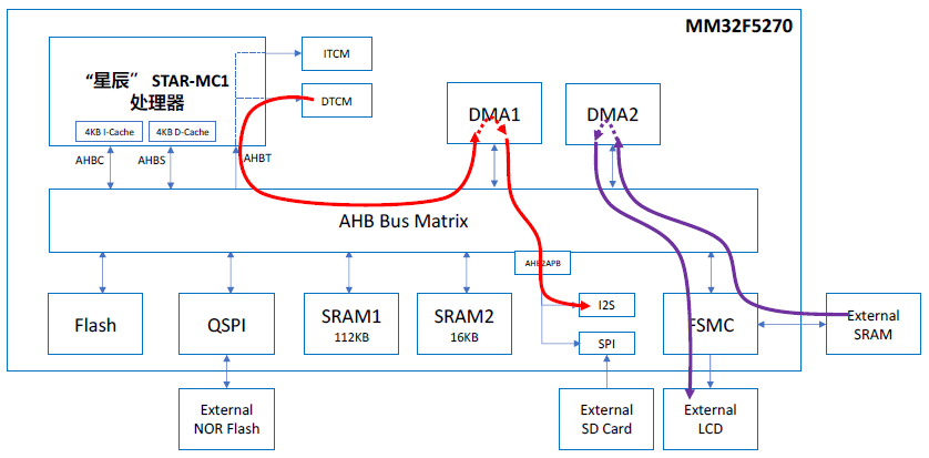
The first part is the CPU processing section.
-
Firstly, the main program executed by the CPU is stored in the built-in 256KB Flash, while the memory needed during operation is stored in SRAM1, as indicated by the blue arrows in the diagram below;
-
At the same time, the CPU needs to read audio files from the external SD card, which involves file system interaction and MP3 software decoding operations, and stores the decoded audio data in 32KB DTCM, as indicated by the yellow arrows in the diagram below;
-
Finally, the CPU needs to run the GUI application, including obtaining display data and font libraries from external Flash, processing them through the CPU, and caching the images to be displayed in external SRAM, as indicated by the green arrows in the diagram below.
The second part is audio playback data stream control.
Here, DMA1 is used to process the audio data stream. DMA1 reads the decoded audio data from DTCM via the AHBT bus and writes it into the I2S TX FIFO, communicating with the external amplifier through I2S to drive the speaker or headphones, as indicated by the red arrows in the diagram below.
The third part is image display data stream control.
Here, DMA2 is used to process the image display data stream. DMA2 reads the images to be displayed from external SRAM via FSMC and writes them to the external LCD screen through FSMC to achieve periodic refresh of image frames, as indicated by the purple arrows in the diagram below.
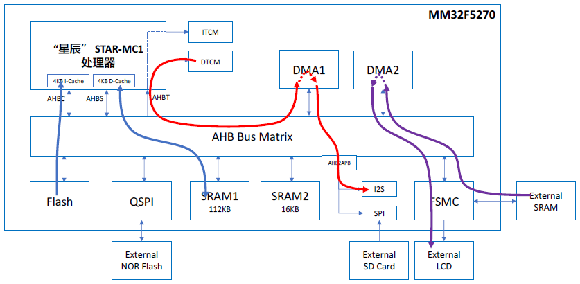
Based on the above analysis, after summarizing all paths and removing non-independent paths (i.e., paths that share common initiators or receivers), we can obtain the summarized data paths as shown in the diagram below. It can be seen that the instruction fetching and execution of the main program (blue arrows), main program data read/write (blue arrows), audio data stream (red arrows), and GUI data stream (purple arrows) are completely independent paths. Assuming the system operates at 120MHz and all accesses use a 32-bit width, it can be calculated that the overall system throughput can reach 15Gbps!
Of course, this is just a simplified example. The actual application may require more complex functionalities. However, the important point is that the multi-concurrent bus architecture of the MM32F5270 provides hardware support for parallel processing scenarios in various practical applications, greatly optimizing the overall system throughput.
It should also be noted that the resources such as SRAM2 and ITCM were not utilized in this example, so they can be used for other purposes, such as SRAM2 for data caching for ENET, USB, CAN, or ADC, and ITCM can store algorithms or interrupt service routines that require real-time performance. If all these functions are developed, can the system throughput be further improved? This question is left for interested readers to ponder 😊.
Summary & NEXT
This article introduced the multi-concurrent bus architecture adopted in the MM32F5270 and illustrated the throughput enhancement effects achievable in practical applications through the example of an audio player with a display.
To be continued! This is the second article in the MM32F5 discussion series, and updates will continue to be shared, aiming to share interesting technologies included in the MM32F5 series. Stay tuned!
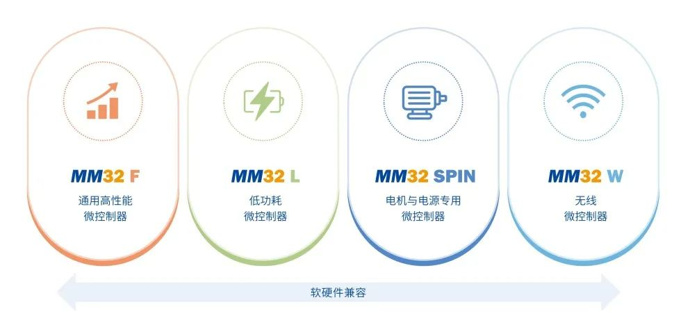
Agile was established in 2011 and is a leading domestic supplier of general-purpose 32-bit MCU products and solutions in China. The MM32 MCU products developed by the company based on the Arm Cortex-M series cores have four major series: F/L/SPIN/W. Currently, more than 200 models have been mass-produced, with cumulative shipments reaching hundreds of millions. Nearly 100 million excellent products equipped with Agile MM32MCUs are delivered to customers every year, ranking among the top in domestic general-purpose 32-bit MCU companies.
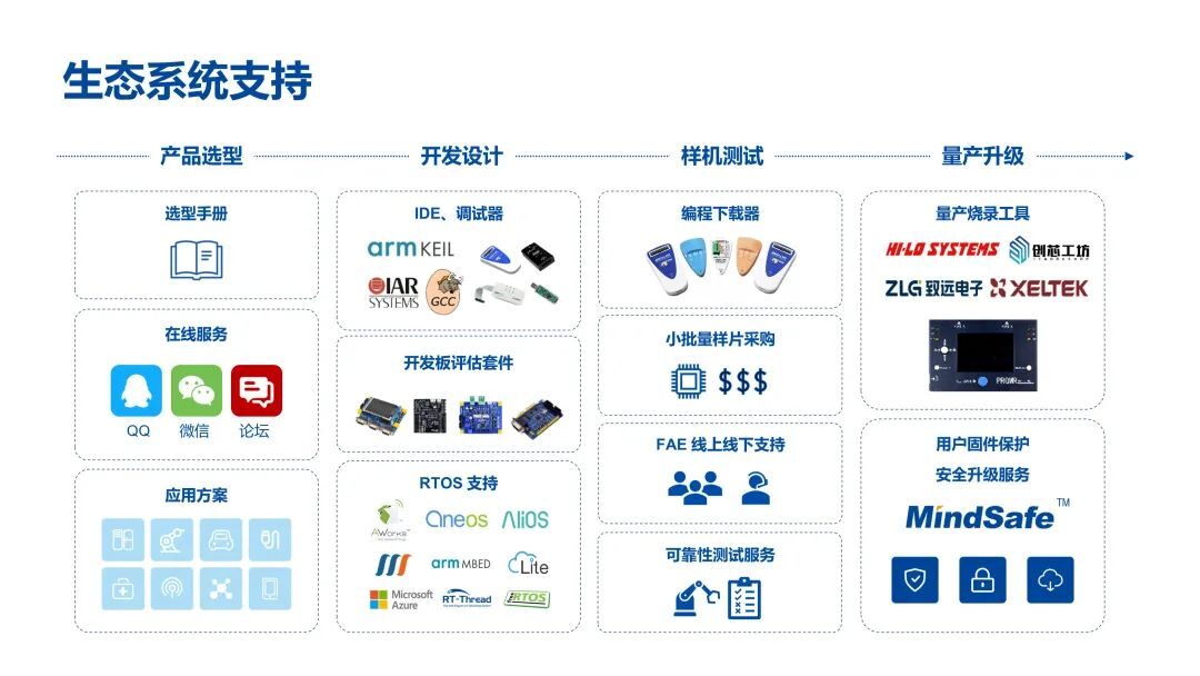
 Agile’s customers cover various application fields including smart industry, automotive electronics, communication infrastructure, medical health, smart home appliances, Internet of Things, personal devices, mobile phones, and computers. Agile Microelectronics is one of the few domestic MCU companies that have received official support from Arm-KEIL, IAR, and SEGGER, establishing a complete general MCU ecosystem to provide comprehensive support for customers from hardware chips to software algorithms, from reference solutions to system design.
Recommended Reading


Technical Sharing | Discussion on MM32F5 Series 1: "Star" Processor?!
Copyright belongs to the original author. If there is any infringement, please contact for deletion.