Click on the blue text aboveComputer Vision Alliance to get more insights
Deep black leather jacket, pale hair.
The familiar Huang has come again, but missing the spacious venue and fan screams.

Due to the pandemic in the United States, NVIDIA, like other tech companies, has changed this year’s GPU Technology Conference (GTC 2020) to an online event.
However, what was unexpected was that this year’s GTC didn’t even adopt a live format, but instead released 7 pre-recorded videos in one go, all recorded in advance by Huang Renxun at home. The level of laziness may only be second to Apple directly launching new products.
Even if Zoom isn’t safe, Huang at least could have used some other software to do a live stream.
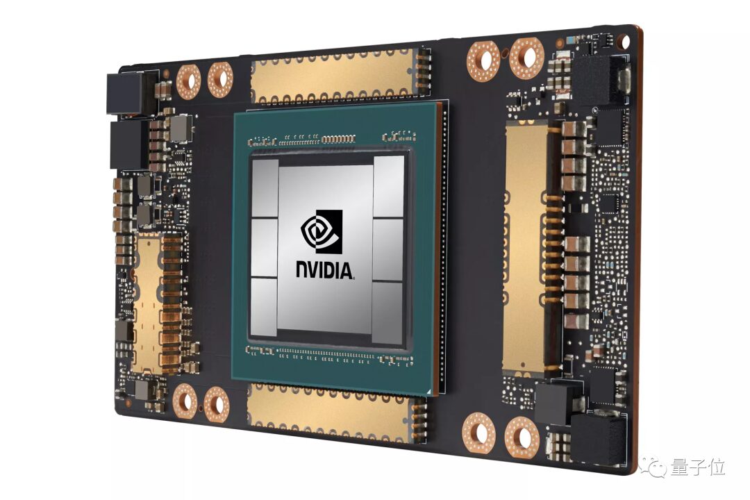
Not sure if he has heard the joke about the 2080Ti gas stove in the player circle, but Huang released a teaser video yesterday: he took out a gigantic device from under his gas stove — a server motherboard equipped with 8 GPUs, claiming to be the world’s largest graphics card.

Is Huang implying that this GPU can get as hot as an oven?
From the size, it cannot possibly be a consumer-grade graphics card, could it be that the RTX 3080 is gone?
Unfortunately, yes.
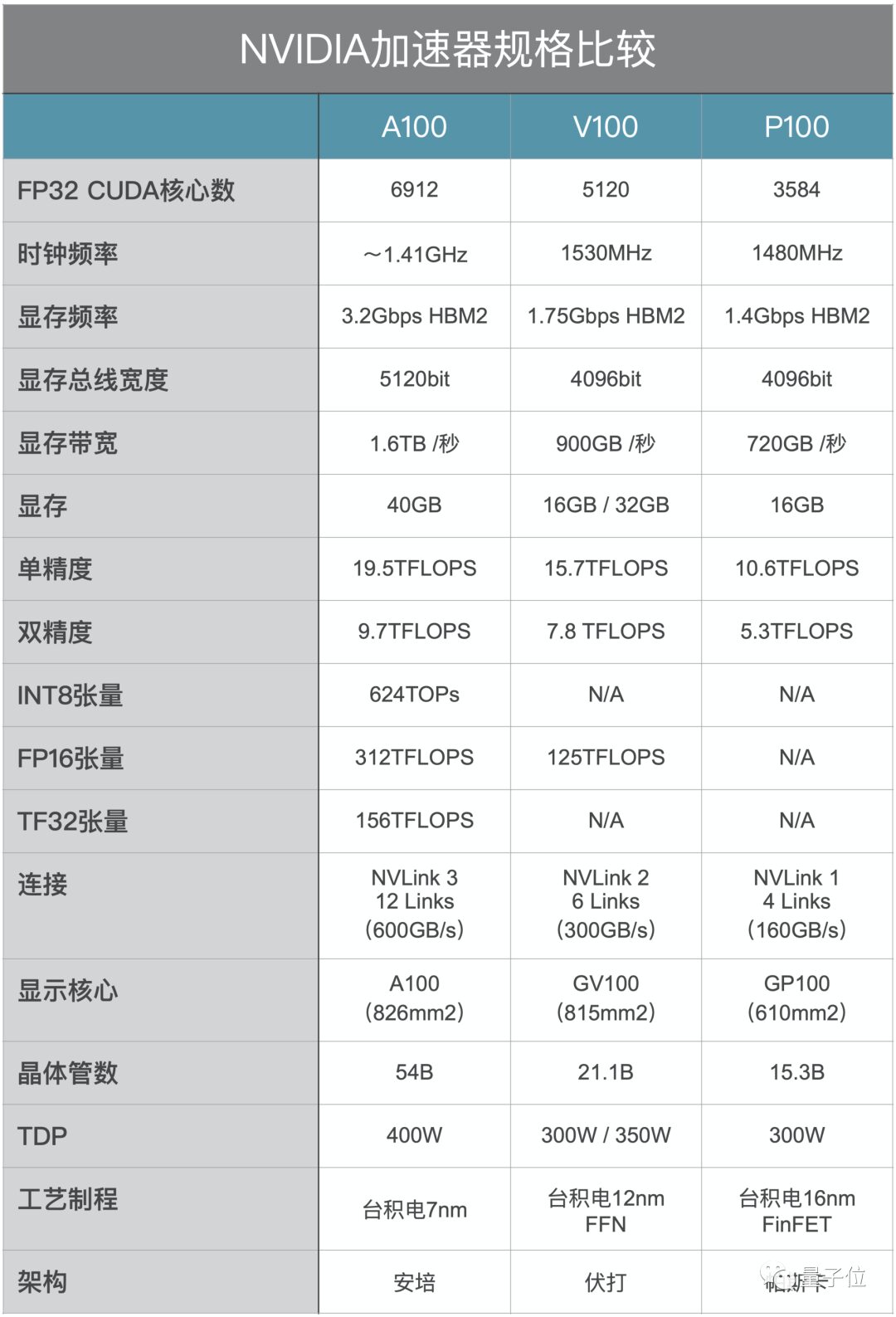
This year’s GTC did not have updates for the RTX series gaming graphics cards. However, the V100, which has been in service for 3 years, welcomed its successor, the all-new professional-grade GPU based on the Ampere architecture — A100. In AI training, one A100 can outperform six others.
This AI computing performance monster further enhances tensor computing capabilities, adding new tensor cores that support sparse tensor computations, making Huang’s GPU seem to be able to be called TPU now.
As for the performance parameters of the A100, let’s start detailing below.
The First Ampere Architecture GPU is Here
The “V” in V100 stands for Volta architecture, while the “A” in A100 stands for Ampere architecture.
The latest A100 GPU integrates over 54 billion transistors, earning it the title of the world’s largest 7nm processor.
Huang explained that such a high level of integration has reached the limits of today’s semiconductor processes; the A100 is the largest processor core ever produced by humanity and also the highest integrated computer processor in history.
NVIDIA has significantly improved the performance of the A100’s tensor cores, achieving an FP32 performance of 19.5 trillion operations per second, with 6912 CUDA cores, 40GB of memory, and 1.6TB/s memory bandwidth.
But with such excellent performance integrated into the GPU, you can’t use it to play any AAA titles.
The A100 itself is not a gaming graphics card. In terms of single-precision and double-precision floating-point performance, the A100’s improvement over the V100 is not significant, but the tensor core’s computing capability has greatly improved, with FP16 tensor performance nearly 2.5 times that of the V100.
Moreover, the V100 has also introduced support for 32-bit tensor floating-point operations (TF32), which can better handle sparse tensors in AI computations.
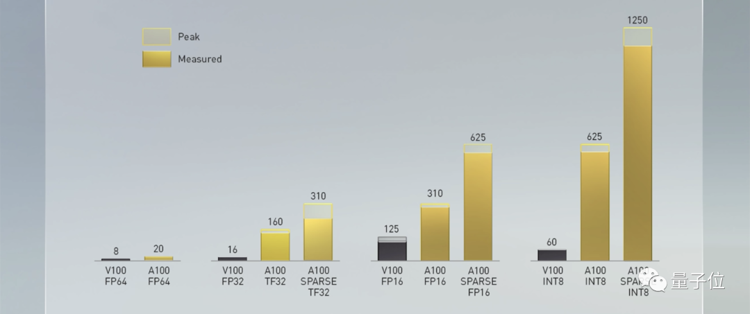
With the optimization for sparse tensors, the A100’s performance in FP16 precision is 5 times that of the V100, while in INT8 it has improved by 200 times!
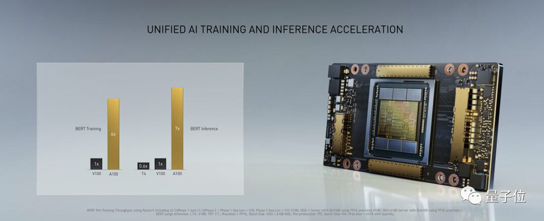
This powerful tensor core has brought a leap in performance for the A100 in AI. Taking the BERT algorithm in the NLP field as an example, the A100 improves training speed by 6 times compared to the V100 and inference speed by 7 times.
 The increase in memory bandwidth is also quite impressive, with multi-layer HBM2 memory providing a total of 1.6 TB/s bandwidth, an improvement of 78% over the previous generation.
NVIDIA will apply the A100 to the stacked AI system, which is the “preheated” GPU board that Huang took out from his oven a few days ago.This brand new stacked AI system is called DGX A100, integrating 8 A100s.

The DGX A100 system can achieve 50 petaflops of floating-point computing performance. This is thanks to these 8 A100s, which use NVIDIA’s third-generation NVLink for integration.
Combining 8 GPUs means there is 320GB of GPU memory and 12.4TB/s of memory bandwidth. The system also includes 15TB of 4th generation NVMe internal storage, providing strong support for AI training tasks.
This system is not cheap, with the DGX A100 priced at $199,000, making it the most expensive “oven” ever.
But Huang is skilled in slicing, previously accurately cutting consumer-grade graphics cards and now precisely “cutting the cake” for the DGX A100.

This slicing technique is called Multi-Instance GPU (MIG), which can divide a single A100 GPU into up to seven independent GPUs.
In other words, researchers and scientists using the DGX A100 system can split tasks into up to 56 instances, distributing many small-scale tasks across the powerful GPUs.
If you can’t afford the A100, no problem, you can find a few people to crowdfund it.
The DGX A100 system has already started selling and will first be applied in the research on COVID-19 at the Argonne National Laboratory in the United States.
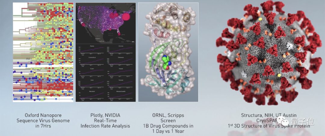
Huang Renxun said: “The computing power of the DGX A100 system will help researchers explore treatments and vaccines and study the spread of the virus, enabling scientists to complete years of AI-accelerated work in months or days.”
In addition to research institutions, NVIDIA stated that large cloud service providers such as Microsoft, Amazon, Google, Alibaba, Baidu, Tencent, Inspur, and Lenovo plan to integrate the A100 into their products.
6 Times Performance Improvement in Autonomous Driving Chips
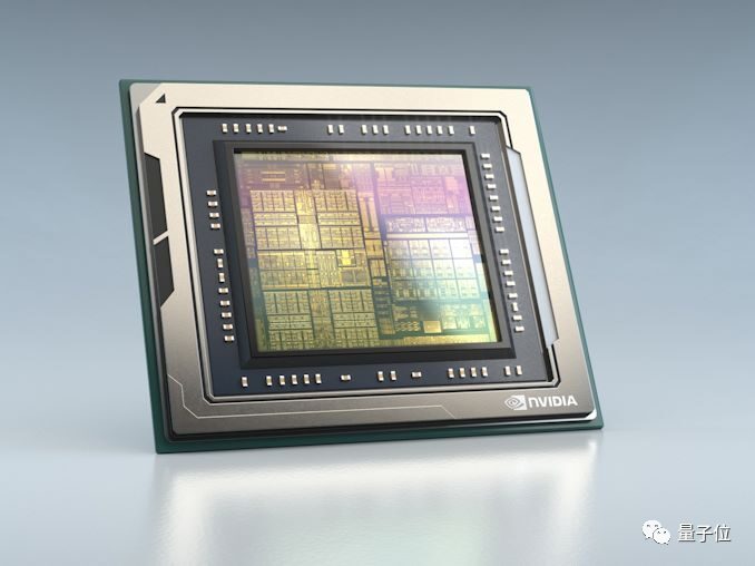
In the keynote speech at this GTC conference, Huang announced the expansion of NVIDIA’s existing autonomous driving platform DRIVEAGX with the upcoming Orin system-on-chip (SoC) series and A100 GPU.
The scope of this expansion covers from ADAS systems to the DRIVEAGX Pegasus Robotaxi platform.
The new DRIVEAGX platform will feature a new type of Orin SoC. Its power is only 5 watts, but its performance can reach 10 TOPS.
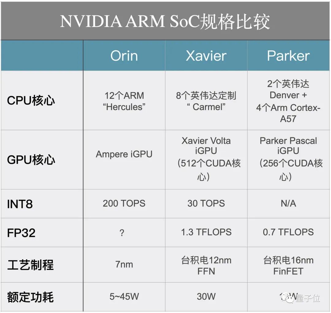
The new platform also achieves 2000 TOPS of performance with two Orin SoCs and two A100 GPUs, meeting the needs for higher resolution sensor inputs and more advanced autonomous driving algorithms.
This architecture represents the largest performance leap in NVIDIA’s autonomous driving SoCs to date, increasing the performance of the DRIVE system by 6 times.
Now, companies such as Pony.ai, Faraday Future, and Canoo have announced partnerships with NVIDIA to use the DRIVEAGX computing platform in their developing vehicles or autonomous driving products.
New Edge AI Chips
This online GTC 2020 also launched two powerful EGX edge AI platform products: EGXA100 for larger commercial general-purpose servers and Jetson Xavier NX for micro edge servers.
 These two products can provide secure, high-performance AI processing capabilities at the edge.
EGX Jetson Xavier NX is the world’s smallest and most powerful AI computing platform, suitable for micro servers and edge intelligent IoT boxes.
The new motherboard looks identical to the Jetson Nano Developer Kit. In terms of connectivity, it still has HDMI and DisplayPort interfaces, four USB 3.0 interfaces, one micro USB interface, and common GPIO interface options. To connect a camera to the system, it is also equipped with two MIPI CSI-2 port connectors.
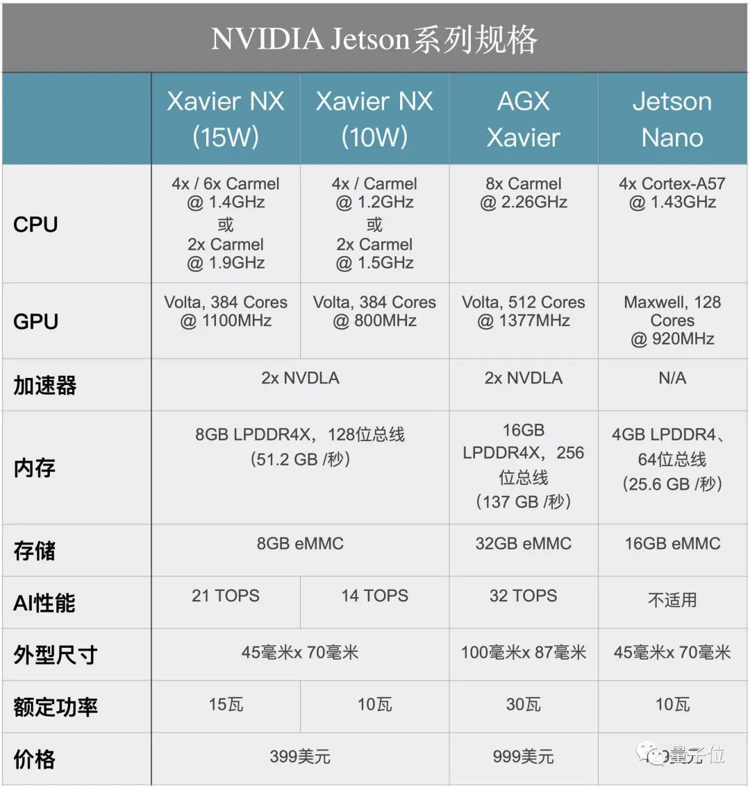
Xavier NX itself is not new, but this time NVIDIA has started selling it in developer kit form, priced the same as the standalone unit, at $399. Compared to the passive cooling solution of the Jetson Nano, the new development kit adopts an active cooling fan.
The platform comes with NVIDIA’s “cloud-native” support, providing solutions for edge AI system deployment, including AI model instances, helping users get started with AI development.
Other Updates
In addition to the A100, autonomous driving AGX, and edge platform Jetson Xavier NX, NVIDIA also launched:
1. GPU-accelerated application framework — NVIDIA Jarvis
2. Open source community collaboration to provide end-to-end GPU acceleration for Apache Spark 3.0
3. Significant performance expansion of the NVIDIA medical platform Clara
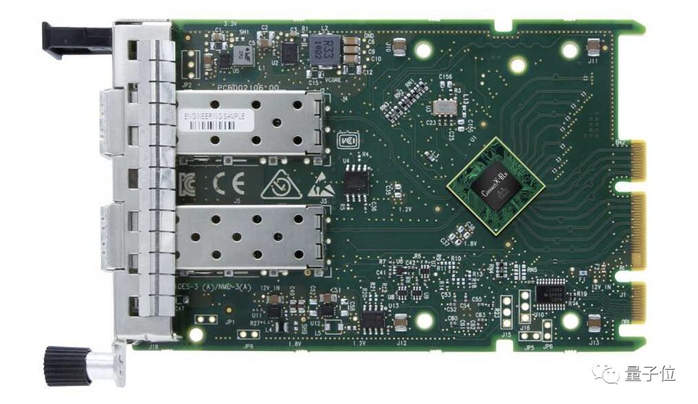
4. 25/50 Gb/s intelligent Ethernet card NVIDIA Mellanox ConnectX-6Lx SmartNIC
What About Gaming Graphics Cards?
This time, NVIDIA did not launch gaming graphics cards, which is actually to be expected.
Huang has always been known for his precise slicing skills; he only released the 20 series Super graphics cards last year, inserting a gap between mid-range graphics cards, and there is simply no motivation to upgrade.
Moreover, using 7nm process on consumer-grade graphics cards will bring a much greater improvement compared to the previous generation’s 12nm process. There have been rumors that the performance of the 3080Ti is 40% better than that of the 2080Ti.
If this is true, Huang Renxun has really squeezed the toothpaste tube dry.
With the Ampere architecture now available, how far can the RTX 3080 be? Furthermore, the performance improvement of the Ampere architecture is so significant that the performance of the next generation gaming graphics cards is highly anticipated!
Reference link:
https://www.youtube.com/playlist?list=PLZHnYvH1qtOZ2BSwG4CHmKSVHxC2lyIPL
end


Doctor’s notes | Zhou Zhihua’s “Machine Learning” hand-pushed notes Chapter 1 Mind Map
Doctor’s notes | Zhou Zhihua’s “Machine Learning” hand-pushed notes Chapter 9
Please support by clicking “View”
