We all know that for mobile processors, the core of their performance lies in the CPU architecture and GPU cores. For example, ARM Cortex A76 is inherently stronger than A75, while Cortex A55 is certainly better than A53. In terms of GPU, Mali-G73MP6 (where the suffix “MP+x” indicates the number of compute cores) outperforms Mali-G72MP6, while Mali-G73MP4 may not be inferior to Mali-G72MP6.
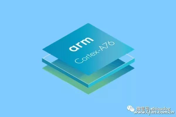
ARM has just released the latest Cortex A76 architecture.
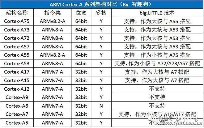
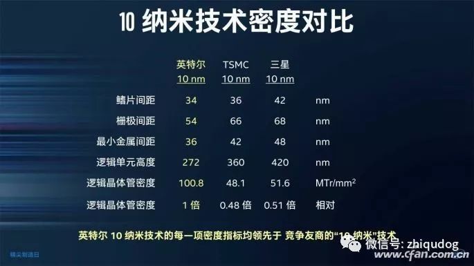
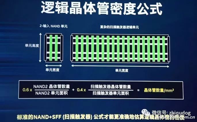
Comparison of ARM A-series architecture parameters.
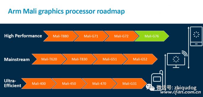
History of ARM Mali series GPU development.
The question arises: when the CPU, GPU, ISP, Modem, and DSP units of a mobile processor are fixed, whether it can exert 100% or even 120% of its strength depends on whether the manufacturing process is compatible.
Back in the day, the Snapdragon 810 had overheating and throttling issues due to the 20nm process being unable to suppress the native Cortex A57 architecture cores, causing problems for many flagship phones.
It can be said that the more advanced the process used by a processor, the more likely it is to appropriately increase the main frequency, generate less heat, consume less power, be less prone to throttling, and run stronger and more stable.
Another question arises: how do we know whose process is stronger?
This is a rather “magical” question because the numbers of the process do not represent everything.
For example, Intel’s 14nm process is equivalent to Samsung’s and TSMC’s 10nm processes, while Intel’s future 10nm process will be more advanced than the other two’s 7nm. Therefore, Intel often claims that its competitors are “not honest” and that their process numbers do not represent the true transistor density.
In fact, Intel is not wrong; it is very “honest” in its approach, continuously refining its 14nm process to 14nm+ and 14nm++ without renaming it to 12nm, which reflects a responsible attitude.
However, Intel always shifts the learning costs onto consumers, making everyone understand that 14nm+ is better than others’ 10nm and 10nm is better than others’ 7nm? It can only be said that the road is long.
As a result, in the eyes of more ordinary users, Intel has been far surpassed by Samsung and TSMC in terms of process technology. By the time Intel mass-produces its first generation 10nm process in 2019, its competitors would have already mass-produced 7nm processes and begun refining their second generation 7nm and 5nm process technologies.
Getting a bit off track, the familiar Qualcomm Snapdragon, Samsung Exynos, HiSilicon Kirin, and MediaTek processors are all manufactured by Samsung and TSMC, so the competition between these two companies’ processes is what we should focus on.
Careful readers will notice that when a new processor is released, manufacturers always highlight that it employs the “X” generation process, and a set of suffixes follows the process, such as 14nm LPE, 10nm LPP, etc.
For TSMC, the most mainstream process currently is 16nm, which TSMC divides into the first generation 16nm FinFET (16nm FF), the second generation 16nm FinFET Plus (16nm+), and the third generation 16nm FinFET Compact (16nm FFC).
The familiar Kirin 95x and Kirin 65x series use the second generation 16nm+. The Kirin 960 (some say Kirin 960 is 16nm+), MediaTek Helio P20/P30/P23, and Spreadtrum SC9860 use the third generation 16nm FFC.
In fact, TSMC has already launched the fourth generation 16nm process, which has been renamed to “12nm”. It is the fourth generation shrink improvement version of the existing 16nm process, and the purpose of changing the name is to counter the advantages of competitors’ 14nm processes, firmly controlling the foundry market between 10-28nm. The 12nm process has already been adopted by new products such as MediaTek Helio P60.
Looks complicated?
TSMC has improved a lot. It should be noted that during the 28nm era, TSMC’s processes were categorized into many versions such as 28LP, 28HP, 28HPL, 28HPM, 28HPC, 28HPC+, etc.!
Currently, TSMC’s latest process is 10nm, which has been adopted by Kirin 970 and MediaTek Helio X30. TSMC is now focusing all its energy on 7nm, and it may no longer release a second generation of 10nm FinFET Plus (the author has not found any information; anyone with insider knowledge is welcome to share in the comments).
Next is Samsung.
Samsung’s mainstream process is 14nm, with the first generation being Low Power Early (14nm LPE), the second generation being Low Power Plus (14nm LPP), the third generation being Low Power Compact (14nm LPC), and the fourth generation being 14nm LPU.
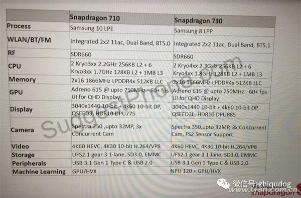
Unfortunately, even the newly released Snapdragon 636 and Snapdragon 632 still use 14nm LPP, while the third and fourth generation 14nm processes are still only heard of but not seen.
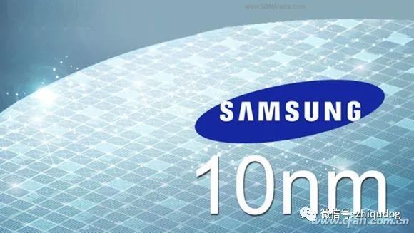
Samsung’s highest-end process is 10nm, which already has the first generation 10nm LPE, the second generation 10nm LPP, and the third generation 10nm LPU, but the LPU process seems not to have been used in any mass-produced chips.
Whether it’s Snapdragon 845, Snapdragon 710, or Kirin 710, they all still use the second generation 10nm LPP. What? HiSilicon Kirin has always been a customer of TSMC, why switch suppliers?
The answer is simple: it is said that TSMC’s foundry costs are high, so Huawei’s wafer foundry business has mostly been transferred to Samsung Semiconductor. Kirin 710 is just the beginning; whether the Kirin 980 at the end of the year will use Samsung or TSMC’s 7nm process is still uncertain.
After reading this article, 99% of readers will also click: