The performance requirements of designers in industrial automation and the Industrial Internet of Things (IIoT) are constantly changing. In terms of microcontrollers (MCUs), they seek faster processing speeds, more memory, better connectivity, and increased security features. At the same time, MCU manufacturers are brewing a new type of MCU to provide designers with a balance between performance, security, and cost.
“As the industrial automation market moves towards Industry 4.0 or IIoT, more sensors, instruments, and other devices are being connected together for data collection and analysis to improve productivity and efficiency in manufacturing plants. Therefore, the demand for more connectivity features in the network is increasing,” said Mamoru Sakugawa, Director of IoT Platform Business at Renesas Electronics. “Due to the different requirements of sensors/networks and targets for different aspects, different communication protocols (i.e., EtherNet/IP, PROFINET, etc.) are needed, so there is currently no single dominant protocol in the market.”
“This drives the demand for higher processing capabilities to seamlessly interconnect all devices without communication delays. With more communication in the network, the need for higher network security also becomes increasingly important,” he added. “All of this will again drive the demand for more embedded memory and SRAM within the system.”
IIoT also presents its own unique requirements around measurement and control, while needing to balance performance and cost.
“Whether as a data communication system or as a specialized term, the Internet of Things continues to become more prevalent. In industrial environments, the growth of IoT is evident as more distributed nodes have varying degrees of autonomy to measure and control parts of processes,” noted Steve Kennelly, Senior Manager of Medical Products at Microchip’s MCU8 Business Unit. “In addition to the ability to communicate via one or more protocols, these nodes also need to achieve an economically viable level of independent real-time control capability.”
Kennelly stated that successful implementation must balance performance, which often means achieving deterministic responses with minimal latency, and costs must also be low enough to enable the scalability required for IoT. “New MCUs are changing the relationship between CPU cores and peripherals by redefining peripherals as easily configurable hardware modules. This provides a very cost-effective platform that can respond to inputs in shorter time frames than CPU instruction cycles,” Kennelly pointed out.
Kennelly mentioned that Microchip’s AVR DA series MCU is an example of a new type of MCU that changes the cost-performance balance for IIoT applications (Figure 1). “It combines the popular 8-bit AVR microcontroller core with peripherals that can operate independently after being configured in software,” Kennelly explained.
“The event system (EVSYS) connects multiple peripherals, so that when one peripheral changes, it can trigger operations of other peripherals without CPU intervention,” he stated. “This allows for the creation of completely deterministic functional blocks, and this is faster than executing code. Graphical tools can easily create arbitrary signal generation, analog signal filtering, custom communication protocols, and more.”
Kennelly noted that the AVR DA MCU can be used in single-chip designs to implement small nodes, such as smart sensors that collect data and send periodic packets over a network. “In more complex systems, such as when each node is a small Linux computer, the AVR DA can be dedicated to implementing certain functions that require fast, deterministic responses,” he added.
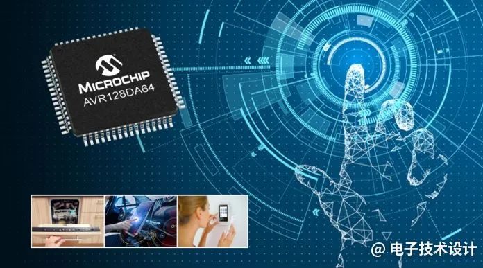 Figure 1:Microchip’s AVR DA series MCU.(Image Source:Microchip)
The AVR DA series MCU is also Microchip’s first functionally safety-ready AVR MCU series with a peripheral touch controller (PTC), enabling real-time control, connectivity, and human-machine interface (HMI) applications. Devices that carry Microchip’s functionally safety-ready designation come with the latest safety features and are supported by safety manuals, Failure Modes, Effects and Diagnostic Analysis (FMEDA) reports, and in some cases, diagnostic software support.
“As functional safety becomes a mandatory requirement in more industrial applications, the AVR DA is also the first AVR MCU to launch with a suite of resources to support multiple standard certification efforts,” Kennelly pointed out.
The AVR DA MCU achieves a CPU speed of 24MHz across the entire power supply voltage range, with memory densities of up to 128KB flash, 16KB SRAM, and 512B EEPROM, as well as a 12-bit differential ADC, 10-bit DAC, analog comparators, and zero-cross detectors. The PTC supports capacitive touch interface designs, enabling buttons, sliders, wheels, touchpads, smaller touch screens, and gesture control for various consumer and industrial products and vehicles. It supports up to 46 self-capacitance and 529 mutual-capacitance touch channels, leveraging the latest generation of PTC with Driven Shield+ and boost mode technology, thus providing enhanced noise immunity, water resistance, touch sensitivity, and response time.
Safety Considerations
While performance is an important factor in choosing an MCU, device safety has become a major concern for industrial OEM designers.
“To have a truly secure processing platform, the processor must not only protect IP from chip-level threats but also ensure protection throughout the lifecycle of IoT devices,” Sakugawa stated. “In short, it must manage different stages of the IoT device lifecycle, known as Device Lifecycle Management (DLM), from design to manufacturing, market introduction, field firmware upgrades, to the end of product life. Each stage requires security measures to ensure information is not leaked.”
Is the chip the first line of defense in device security? “The first layer must always come from the system implementation, namely the IoT device itself,” Sakugawa pointed out. “If the system is not implemented correctly, it is vulnerable to attack threats and potential chip-level threats, which should be the last line of defense. Therefore, secure implementation is not just about chip-level implementation.”
Kris Ardis, Executive Director of Maxim Integrated (now ADI) Micro, Security, and Software Business, stated that the first line of defense must come from awareness.
“The first line of defense is understanding the threats that applications may encounter,” Ardis believes. “While I firmly believe that security should start from the chip as the root of trust for any embedded application, if designers do not consider threats and inadvertently open backdoors, even my most secure MCU will not help.”
“Although we have been promoting highly secure solutions due to our background in providing financial and government-level security solutions, it wasn’t until recent years, with widely known attacks like Mirai and Stuxnet, that we began to see our customers pay attention,” Ardis stated. “We integrate proven cryptographic engines, secure bootloader technology, and high-quality random number generators into most of our MCUs for industrial and medical markets.”
“IoT indeed implies that devices are distributed without restriction, making them more attractive to attackers. The success or failure of an attack is always related to risk—if a device is easy to steal, then the risk of an attacker gaining physical access is very low,” Ardis pointed out.
“This means we need to pay more attention to the attacker’s ability to perform operations such as extracting code or key information,” he added. “In higher-value applications, if an application can sense that someone is attempting to breach it, we may even see the adoption of active tamper detection techniques to erase sensitive information.”
But top-notch security features will depend on the application. “Products in the financial terminal space offer very advanced security features—utilizing low-power, always-on sensors to monitor various attacks. Other technologies like PUF (Maxim offers a physical unclonable function (PUF) implementation called ChipDNA) help provide superior key protection without a battery,” Ardis said.
Ardis stated that these technologies do come with costs, but there are many other techniques available to help defend against various attackers. “Good secure boot methods can thwart many attackers and protect our IP from modification or discovery,” Ardis said.
Performance + Security
Maxim Integrated has recently begun to introduce Error Correction Code (ECC) technology into its MCUs to enhance reliability. “As our embedded MCUs adopt increasingly advanced process technologies, memory (especially SRAM) becomes more susceptible to interference from energy particles. Effectively using ECC can reduce the failure rate from one bit failure every few months to one failure every century,” Ardis stated.
“We are also seeing an increasing industry need for more powerful MCUs—more memory allows for more complex decisions to be made at the edge, thus reducing the need for wireless or wired communication (which has become capacity-limited in many environments), and the power consumption required for local decision-making is also lower,” he stated.
Maxim’s MAX32670 low-power Arm Cortex-M4 MCU is an example of a device that balances performance and security (Figure 2). This MCU includes ECC-protected memory, secure bootloader, and encryption support to help IoT and industrial applications achieve longer lifetimes in harsh environments and extreme power constraints.
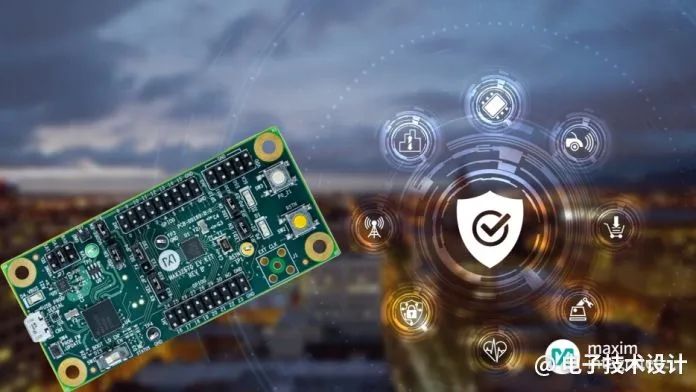 Figure 2:Maxim Integrated’s MAX32670 low-power Arm Cortex-M4 MCU.(Image Source:Maxim Integrated)
In addition to integrated ECC-protected memory, the MAX32670 features low power consumption and small size, saving 40% power and 50% space. This MCU is designed for industrial, healthcare, and IoT sensor applications, with a running power consumption of just 40µW/MHz, making it the lowest power solution for battery-powered sensor applications and 50% smaller than its closest competitor, with packaging options including ultra-small 1.8mm×2.6mm WLP and 5mm×5mm TQFN.
MAX32670 protects the entire memory space (384KB flash and 128KB SRAM) with ECC to prevent bit flips and improve reliability. “As MCU processes shrink to 40nm and below, bit flips become a critical reliability issue,” Ardis pointed out. “With ECC, hardware can detect and correct single-bit errors, making bit flip errors difficult to negatively impact applications.”
Another MCU series that balances functionality and security is Renesas Electronics’ 32-bit RX72N and RX66N MCUs (Figure 3). Targeting industrial automation applications, the MCUs combine device control and networking capabilities on a single chip while enhancing functionality and security features.
For IIoT and industrial automation, Renesas focuses on three areas—real-time performance, multifunctionality for miniaturization of industrial devices, and support for industrial networking, Sakugawa noted.
In the industrial equipment market, improvements in performance and functionality lead to larger program code sizes. Therefore, memory storage capacity and read speeds play a crucial role in determining real-time performance,” he noted.
“In recent years, most industrial automation products have been connected to networks and equipped with many functions, such as LCD panels. However, in many cases, additional MCUs and memory are needed to support network connectivity or extra functions without sacrificing critical features,” he stated.
“On the other hand, devices need to be miniaturized, and these conflicting demands are becoming a challenge in designing new devices. Therefore, we need to achieve single-chip processors with higher performance multitasking processors, larger embedded memory, I/O pins, and other critical peripheral features to minimize BOM (Bill of Materials),” he added.
The Renesas MCUs are built around the company’s RXv3 CPU core, operating at a frequency of 5.82 CoreMark/MHz. The RX72N has a maximum operating frequency of 240MHz, providing 1396 CoreMark and two Ethernet channels, while the RX66N offers a maximum operating frequency of 120MHz, with 698 CoreMark and one Ethernet channel.
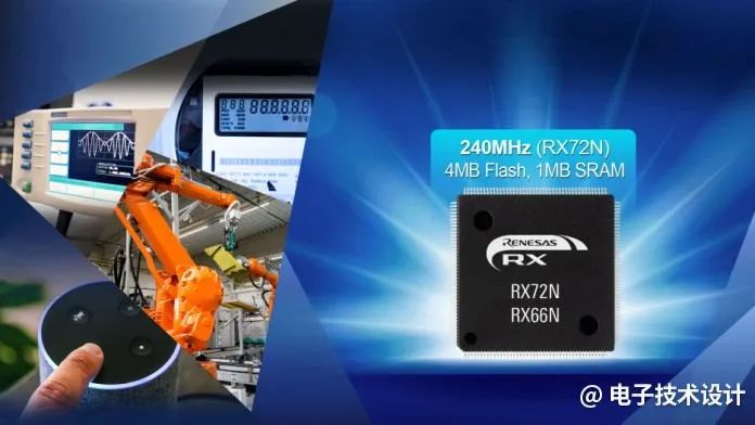 Figure 3:Renesas Electronics’ 32-bit RX72N and RX66N MCUs.(Image Source:Renesas Electronics)
These devices offer up to 4MB of on-chip flash memory, executing read operations at the industry’s fastest frequency of 120MHz, and providing 1MB of on-chip SRAM. With this on-chip memory, there is no need to use slower external memory, thus fully utilizing CPU performance. Larger memory capacity also enables high-resolution graphics support on a single chip, such as WVGA, which was not possible on earlier general-purpose MCUs.
“The RX72N and RX66N products feature the industry’s largest memory capacity—4MB flash and 1MB SRAM. This ensures ample space for user applications as well as previously stored data in external flash memory (e.g., LCD image data),” Sakugawa stated. “Using a large amount of SRAM and processing LCD image data in a two-layer configuration can achieve smooth display performance.
“These products also offer packages with up to 224 pins. This allows for many functions to be implemented without external memory or sub-MCUs, resulting in better performance compared to previous products while also helping to reduce component count, PCB size, and development time,” he added.
These MCUs enable single-chip device control and networking capabilities, enhancing real-time performance for applications such as industrial robots, general inverters, programmable logic controllers (PLCs), and remote I/O devices.
These devices also include hardware accelerators for fast motion control. Arithmetic units for trigonometric functions (sin, cos, arctan, hypot, limited to RX72N) can accelerate motor vector control, while a register group save function can reduce interrupt response time. This reduces CPU load required for closed-loop control and simplifies the implementation of additional functions such as networking.
These MCUs also integrate LCD controllers, 2D graphics engines, and serial audio interfaces. They support high-resolution displays—WVGA (800×480) in 8-bit color or WQVGA (400×240) in 16-bit color—without external memory. When combined with speech recognition or noise reduction middleware, they also enable customers to add voice control capabilities to their products, making them ideal for applications such as networked controllers or smart speakers equipped with LCDs.
In addressing security concerns, these MCUs are also equipped with high-security IP—Trusted Secure IP (TSIP), which supports various encryption engines and key management to prevent hackers from tampering with and intruding upon the MCUs over the network, Sakugawa stated.
The Trusted IP module serves as a security engine to support multiple encryption standards, including AES, 3DES, RSA, ECC, SHA, and TRNG, as well as key management. Combined with the protection features of on-chip flash memory, support for secure firmware updates and secure boot functionality can be provided.
“In any implementation, the security of the system is always driven from its roots, in this case, the brain of the system, which is used to store processing algorithms and important data. Losing control means losing control over the entire system. This is why security must start at the chip level. If our chips are vulnerable to threats, we will completely lose control over the system,” Sakugawa stated.
“In the RX Trusted Secure IP, there is a 128-bit unique ID and TRNG that allows for secure generation and management of keys within the TSIP,” he added. “The TSIP has also passed NIST CAVP (Cryptographic Algorithm Validation Program) certification, which is a truly secure algorithm that provides a root of trust within the chip.”
Additionally, IAR Systems has released new versions of its security development tools, C-Trust and Inception Suite, which expand support for many Renesas MCUs, including the RA and RX MCU series. This support has now extended to RX72N.
C-Trust is an extension of IAR Embedded Workbench that enables developers to protect existing or new applications without having to master the complexities of security. It provides protection against IP theft, malware injection, counterfeiting, and overproduction.
The Inception Suite for implementing and customizing security in embedded applications integrates C-Trust with other security development tools and training to support companies that need to meet legislative requirements, such as California and Oregon consumer laws, ETSI TS 103 645 standard, and IEC 62443 industrial IoT security standards.
Another MCU that meets the security demands and high-performance requirements of IoT is STMicroelectronics’ ultra-low-power STM32L5x2 MCU, which can better protect IoT-connected applications (Figure 4). These controllers provide proprietary security based on Arm TrustZone technology (and are PSA certified level 2), as well as secure boot, complete hardware isolation, and encryption accelerators.
The STM32L5 MCU’s security foundation operates at a clock frequency of 110MHz, starting from hardware-based security based on Arm TrustZone. ST states that designers can include or exclude every I/O, peripheral, or area of flash or SRAM within the TrustZone protection range, allowing for complete isolation of sensitive workloads for maximum security.
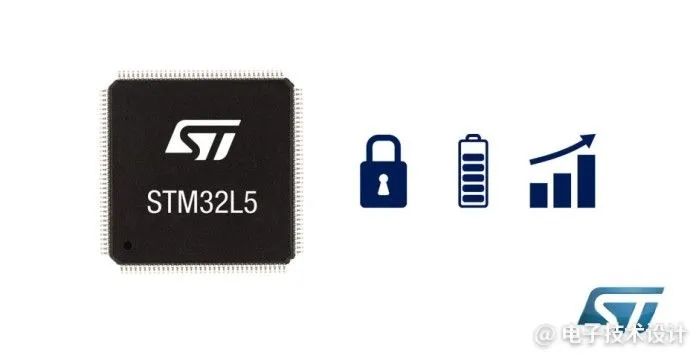 Figure 4:ST Ultra-Low-Power STM32L5x2 MCU.(Image Source:ST)
The company states that it has designed TrustZone to ensure support for secure boot, integrated SRAM and flash with special read/write protection, and encryption acceleration, including AES 128/256-bit key hardware acceleration, public key acceleration (PKA), and AES-128 on-the-fly decryption (OTFDEC) for protecting external code or data. The STM32L5 also supports active tamper detection and secure firmware installation.
The company also provides designers with a comprehensive set of network protection resources for IoT design, called STM32Trust. Tools, evaluation references, and source code are now available for free download.
ST has not overlooked the need for IoT applications to reduce power consumption. The STM32L5 combines technologies such as adaptive voltage regulation, real-time acceleration, power gating, and various low-power operating modes, enabling the MCU to provide high performance and long run times whether powered by button batteries or through energy harvesting. Additionally, it can instantaneously power on or off a highly efficient switching mode buck regulator to improve low-power performance when VDD voltage is sufficiently high.
Moreover, the STM32L5x2 MCU provides 512KB dual-zone flash memory, allowing read/write operations to assist in device management, and supports ECC with diagnostic capabilities. There is also a 256KB SRAM and functionality supporting high-speed external memory, including single, dual, four, or eight-line SPI and Hyperbus flash or SRAM, as well as interfaces for SRAM, PSRAM, NOR, NAND, or FRAM.
Author: Pablo Valerio, Source: EDN sister site Electronic Products
Reference Original:
MCUs Address Industrial Automation and IIoT Challenges, compiled by Franklin Zhao.
Copyright Notice: This article is from the August 2022 issue of “Electronic Technology Design” magazine, all rights reserved, no reproduction without permission.
♥Click 👇 Business Card, Follow Me♥
1. Huawei Genius Youth Used 108 Days to Type a Character, Redefining Customized Keyboards
2. Disassembling a Chinese-made “Raspberry Pi” Development Notebook, Is the $279 Price Worth It?
3. Domestic Replacement MCU Pitfall Records