
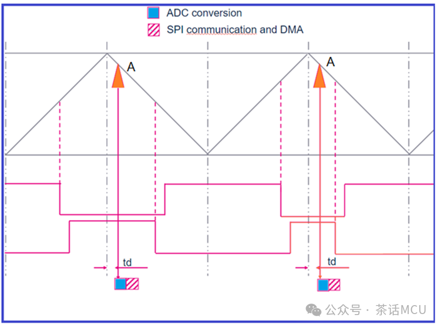
Currently, there are STM32 users developing products using the STM32G474R chip, where TIM1 is used for power drive, with TIM1 operating in center-aligned counting mode. There is a demand to trigger external ADC device sampling at the moment indicated by the arrow in the figure below during each cycle of TIM1. After the ADC completes the conversion, the results should be retrieved via the SPI interface. However, there is a requirement that the process from the triggering moment [point A in the figure below] to retrieving the ADC results should not involve the CPU.
The user believes that the principle is feasible, but after some struggles, they feel that the implementation of the corresponding hardware timing and DMA transfer has encountered some obstacles. It’s like solving a Rubik’s cube; the rules and requirements are clear, and the basic actions are simple, but achieving success is not easy.
Let’s take a closer look at the current ADC device used and its associations and requirements with the STM32G4 in terms of hardware timing. The yellow bar in the figure below records several signals used by the external ADC device, while the green bar records the signals or pins connected to the STM32G4 chip. The red signals in the figure represent those sent from the ADC device to the STM32, while the blue signals are sent from the STM32 chip to the ADC device.
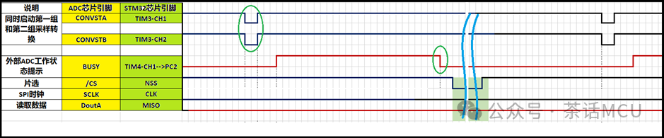
The current timing requirement is that at point A of each counting cycle of TIM1, the STM32 first generates two ADC start signals, which are the two falling narrow pulses in the above figure. After the ADC conversion is complete, the STM32 should start receiving multiple data based on the falling edge of the ADC device’s BUSY signal, which clearly requires the involvement of DMA.
The question now is, how to synchronize and associate point A with the ADC start signals? How to generate those two start pulses? Then, after the ADC conversion complete signal appears, how to relate it to the SPI reception on the STM32 side? Remember, the whole process should not involve the CPU.
I will provide a solution for reference. Since the following verification test is based solely on the STM32G4 chip itself and does not connect to the corresponding ADC device, I simulated the generation of the ADC device’s Busy signal with the STM32G4 chip. Additionally, I used SPI1 and SPI2, where SPI1 acts as the master SPI on the STM32G4 side, responsible for reading results from the external ADC device. SPI2 simulates the ADC device’s slave SPI to send results to the STM32G4 chip.
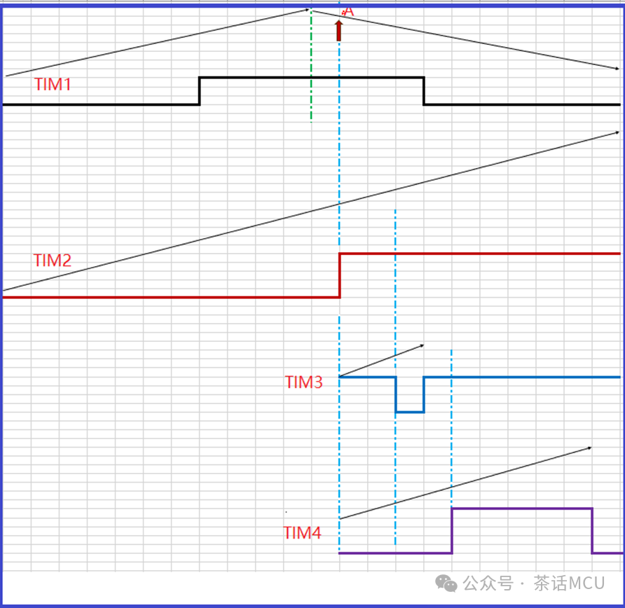
I synchronized TIM2 with TIM1 and set the same counting period. When TIM2 counts to the point corresponding to TIM1‘s A point, it generates an OC1 event to synchronize and start TIM3 and TIM4. TIM3 outputs two ADC start pulses based on two channels and then stops, while TIM4 is used to simulate generating the BUSY signal of the ADC device. The BUSY signal is connected to the PC2 pin of the STM32G474RE chip, and the falling edge-triggered external interrupt event based on PC2 serves as a synchronization signal for SPI1‘s DMA transmission.
I have illustrated the content described above in the figure below, showing the timing relationship of various signals from point A to the generation of the Busy signal, making it easier to observe and understand. Specific parameters can be adjusted according to actual conditions.
To generate this timing relationship, the core knowledge points required are the master-slave triggering and synchronization of TIMER and the characteristics of different output comparison modes of TIMER, which should be effectively utilized.
After solving the timing relationships between the previous signals, we still cannot rest easy. We also need to have a clear understanding of the principles related to DMA and DMAMUX, as well as the knowledge points related to SPI applications to solve the current problems.
Next, I will paste all the configurations and user code for reference; I won’t be able to explain each line here.
Once the principles are clear, we can use the STM32 development tool – STM32CubeMx graphical tool for initialization configuration. By the way, the solutions mentioned here are not set in stone; as long as they achieve the goal, they are acceptable. Especially regarding the specific implementation of the TIMER, it is often flexible and diverse.
1. Configuration of TIM1. It is not the focus here; the main task is to construct a secondary timer 2 that starts synchronously based on it. The main task of TIM1 is to perform its driving function.
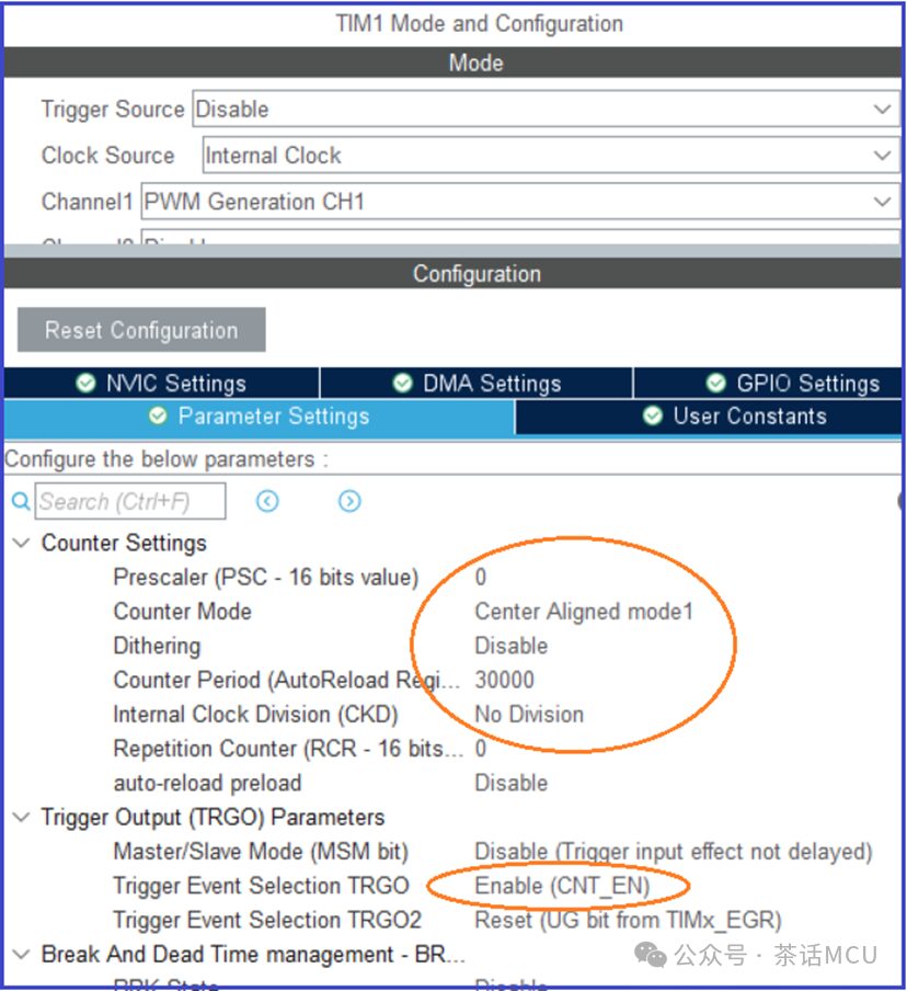
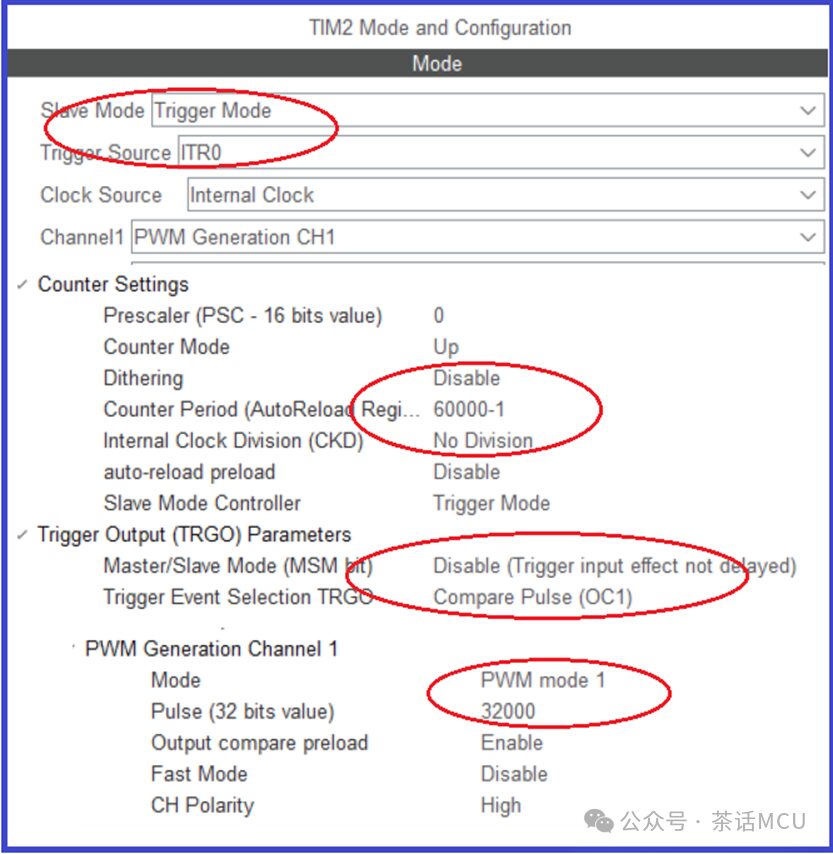
2. Configuration of Timer 2. It is triggered and started by TIM1. The counting period is the same as TIM1, and it generates an OC1 comparison event at a specific counting point [the position corresponding to point A mentioned earlier].
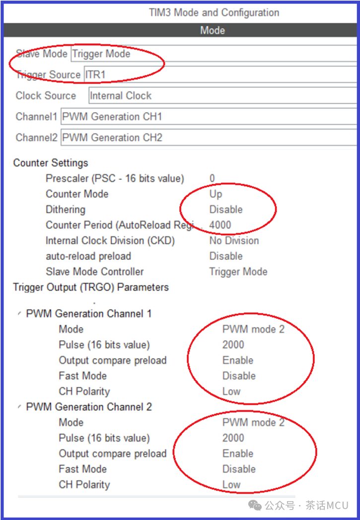
3. Configuration of Timer 3, which is triggered by TIM2 and operates in single pulse mode. The counting period is determined based on its own signal characteristics and timing requirements. Channels 1 and 2 are used to generate two identical ADC start signals.
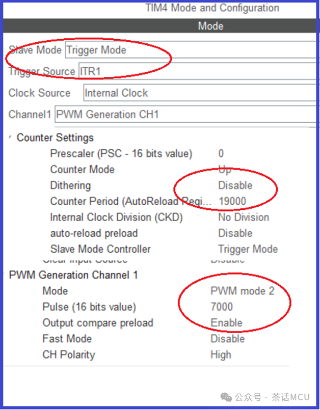
4. Configuration of Timer 4, which is also triggered by TIM2 and operates in single pulse mode. The counting period is determined based on its own signal characteristics and timing requirements. Here, channel 1 is used to simulate generating the BUSY signal of the ADC device.
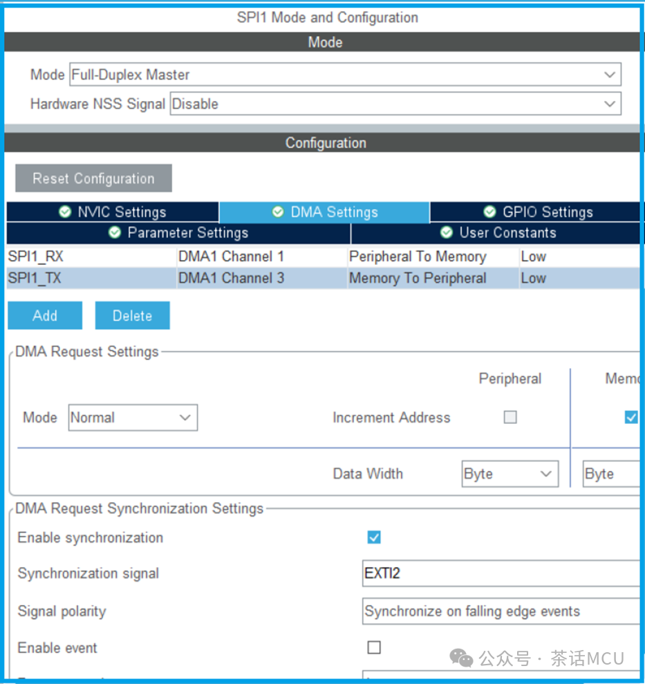
5. Configuration of SPI. SPI1 acts as the master device, responsible for reading results from the ADC device to RAM. SPI2 simulates the slave device of the ADC, responsible for sending ADC results to the master device. I enabled DMA transmission for receiving and sending on SPI1, and the DMA sending uses the EXTI2 event for synchronization. Additionally, I also enabled the DMA sending function for SPI2. The focus here is on the DMA configuration of the sending function of SPI1.
The basic configurations that need to be focused on are these; other configurations related to clocks and EXTI2 will not be included. After creating the project, add user code. The user code to be added here is relatively simple. See the figure below, which consists of a few lines of startup code.
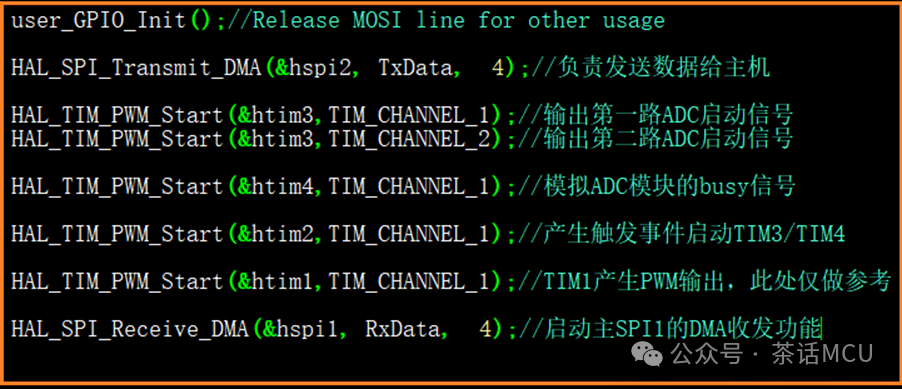
Since only data needs to be received here, it doesn’t matter if the MOSI pin is released, which is why the first line of the screenshot above is not a focus. The following figure shows the actual waveform during my verification test:
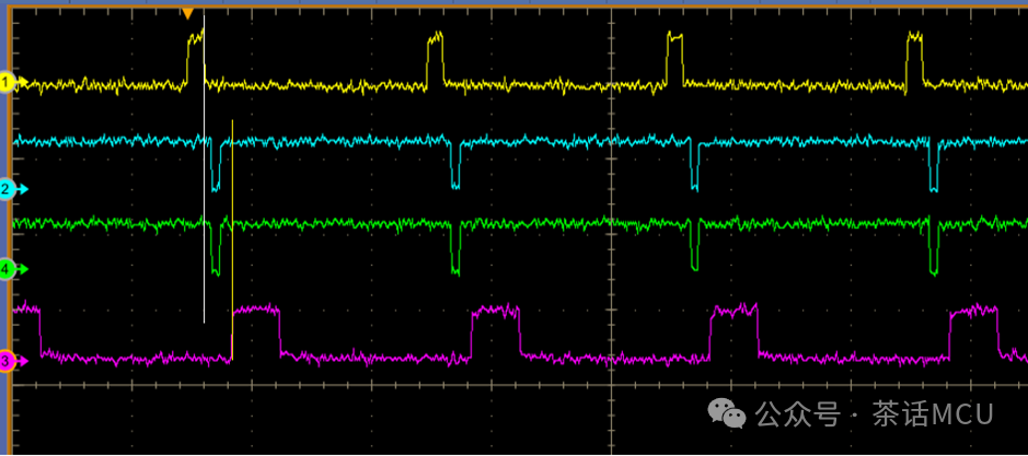
The yellow waveform in the figure above is the output waveform of TIM1. The two green waveforms are the start signals sent from the STM32G4 to the ADC device. The purple waveform is the simulated BUSY signal generated by the STM32G4.
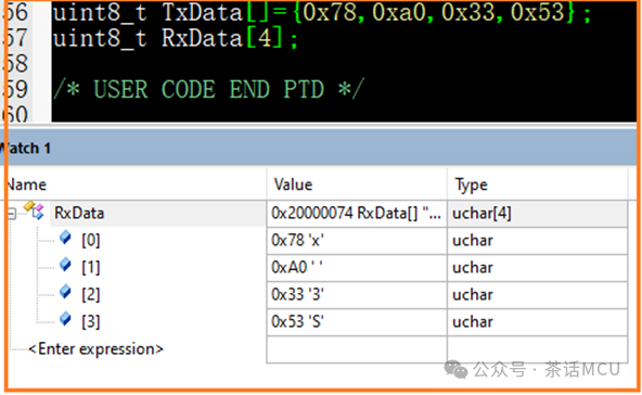
Let’s take a look at the verification results based on the configurations and code above. Each time, 4 data points are read back. The following two images are screenshots of two different simulation test results. TxData is the data sent from SPI2, while RxData is the data received by the master SPI1.

Alright, that’s all for today’s topic. I hope it can provide some reference and inspiration to everyone. The content above involves a lot of things and is quite comprehensive, and the application is also flexible. If there are any related questions, we can discuss and communicate!
~~~~~~~~~~~~~~~~~~~~~~~~~~~~~~~~~
Previous topic reading links:
1. The topic of jumping between different program areas of the STM32G4 chip
2. Several situations that may be encountered when triggering ADC with a timer
3. Why are 2 data lost during SPI transmission?
4. Example of implementing STM32 HRTIM Burst output mode
5. Why can’t UART send new data after enabling Cache