 1. Determine the Plan and Purpose
Hello everyone, today the miniaturized development board has arrived, and we are starting the arrival inspection task. The requirements are as follows:
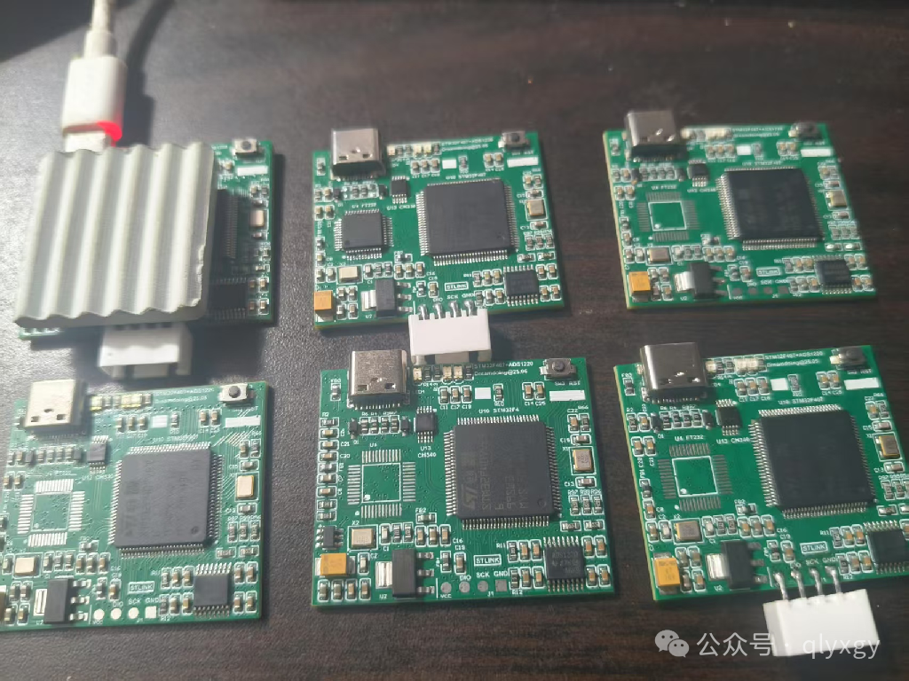
[Notes] STM32F4 + FT232H High-Speed Acquisition Development Board Design Draft
Objective: STM32F4 Development Board 01. High-speed transmission testing, and reliable verification; 02. ADS1220 driver verification and debugging; Keywords: PCB, STM32F4 Note: High-definition images can be viewed via WeChat on mobile phones.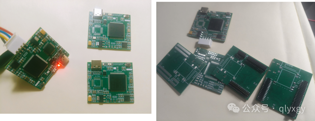 2. Basic Testing Content
01. The FT232H chip needs to be configured for high-speed FIFO mode. After configuring the mode, send the AC3 clock, then switch the data via the parallel port;
02. Load data at high level with AC3, then trigger a low level to complete one FIFO load;
03. The FIFO function generates a cache after enabling reading in the DLL file, and after completion, the API interface outputs and releases the cache;
04. There may be a persistent waiting phenomenon when calling the DLL interface, which needs subsequent optimization to resolve;
06. The FT232H chip has internal and external power configurations, and there will be heating phenomena in high-speed FIFO mode. It is recommended to add heat dissipation measures under high conditions;
07. The STM32 writes a test program to drive, outputs the clock, then switches the parallel port for testing;
08. The parallel port function needs to meet the requirements for fast transmission, and under controllable speed, single IO operations can be used;
 3. Communication Testing Content
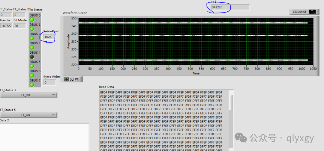 01. Write a program to receive data on the computer, receiving 1024 data points each time, with a 20ms interval, testing 342,000 times;02. Total time spent: 342,000/50/3600=1.9 hours;;03. Total data volume =342,000*1024=35020.8 million=350 million data points, tested successfully;04. Verification result: It can meet the requirements for high-speed transmission and different rate transmission needs;05. During high-speed transmission, the system consumes about 50mA under 3.3V power supply, and the chip exhibits heating phenomena;06. The function of the STM32 program is: output three pulses to send three values, sending in a loop;07. Configure the transmission chip to FIFO mode, then download and save parameters;
 4. ADS1220 Chip Testing
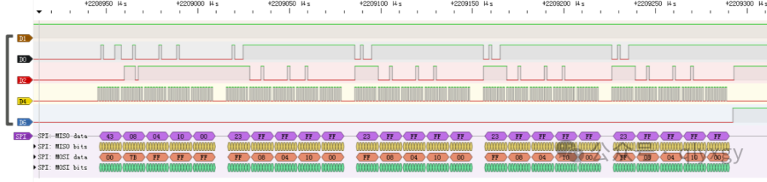
Description of Phenomenon: Unable to operate the register
01. After writing to the register with 0x43, reading the register with the 0x23 instruction responds, but all values are default 0x00;
02. The 0x06 instruction works normally, and the RDATA instruction can also read data;
Solution:
01. Suspect that the SPI bus level is mismatched; the oscilloscope verifies that the levels are normal, and data feedback is also normal;
02. Suspect that the CS and ready signals are not ready before operating the register; added delay and analyzed with a logic analyzer, signals are normal;
03. Suspect hardware chip damage, or bus interference or disconnection; RDATA has data feedback, indicating the chip is normal, and circuit routing is normal;
04. Suspect GPIO conflicts and configuration issues; determined through a logic analyzer that the configuration is normal and without conflicts;
05. Suspect SPI bus configuration issues; discovered through a logic analyzer that the clock phase was incorrect; checked SPI configuration and changed the first edge to the second edge, which worked normally; retested data with a logic analyzer, and it was normal;
 5. Schematic and PCB
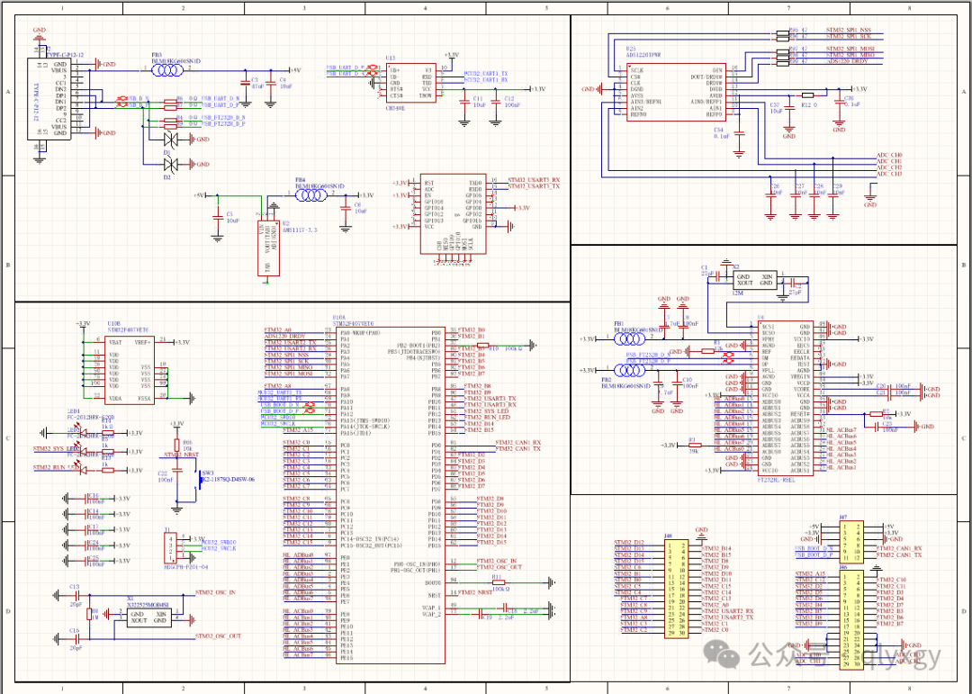
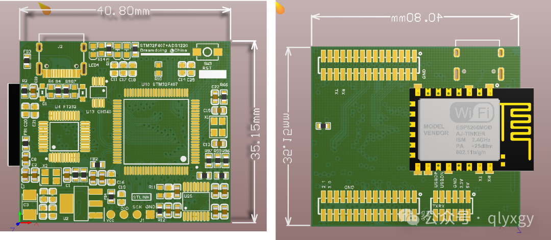 01. Power supply voltage regulator chip with magnetic beads + filter capacitor design; USB adds ESD/TVS protection bidirectional diode devices to protect against static interference;03. Circuit power consumption calculation: STM32F4 + FT232H + ADS1220 + CH340 + ESP8266, calculated under normal maximum load will not exceed 0.6A;04. The 3.3V voltage regulator chip has heating phenomena; attempts to solve this with a heat sink; need to check installation height;05. Four-layer board design verifies that signal transmission is normal, downloads normally, serial port is normal, SPI bus is normal;06. [Planning 01] Design acquisition carrier board, enabling ADS1220 low-speed high-precision 24-bit analog acquisition branch;07. [Planning 02] Design acquisition carrier board, enabling AD7606 high-speed 8-channel acquisition branch;08. [Planning 03] Design control carrier board; exit the core board product;6. Statement01. All codes, images, and text in this tutorial are original, and the copyright belongs to Qianli Youxuan Teaching Base;02. This tutorial is for technical sharing, applied in the teaching field; related codes and technical discussions are for reference only;03.Note: High-definition images can be viewed via the mobile WeChat client.;