1. What is a Clock Signal
The clock signal (Clock Signal) is the foundation of sequential logic, used to determine when the states in logic units are updated. It is a signal with a fixed period that is independent of operation. The clock signal has a fixed clock frequency, which is the reciprocal of the clock period. It has only two levels: low level and high level. The high level can vary according to circuit requirements; for example, the TTL standard high level is 5V. The most common duty cycle for clock signals is 50%, meaning that the duration of the high and low levels is the same.
The clock signal for STM32F103C8T6 is generated by an external crystal oscillator (or an internal RC oscillator circuit of the microcontroller), which can provide a very stable and precise frequency. Generally, we should use an external clock, as it is more stable and accurate than the internal clock.
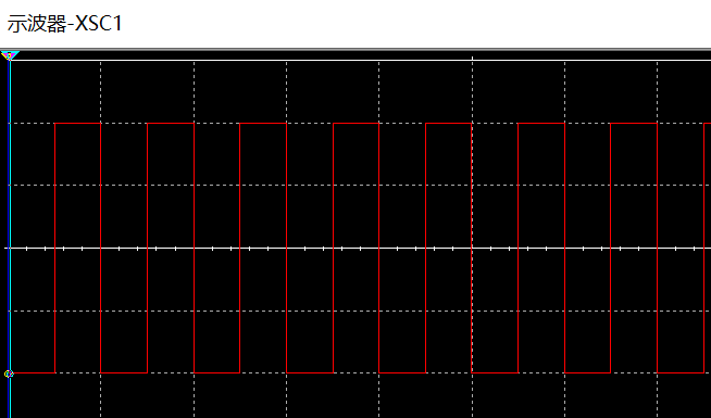
The following figure shows the clock signal observed on an oscilloscope:
2. What is the Use of Clock Signals
Why Do Microcontrollers Need Clock Signals
We can directly search on Baidu, and there are various answers, but to summarize, they are as follows:
Synchronization: Microcontrollers consist of thousands of small circuits, including logic gates, registers, counters, etc. All these circuits need to operate in a strict time sequence. The clock signal provides a synchronized pulse for these circuits to ensure they work together correctly.
Instruction Execution: Each instruction execution in a microcontroller requires a certain number of clock cycles to complete. The clock signal determines the execution speed of the instruction and the overall program running speed.
Data Transmission: When the microcontroller communicates with external devices or other microprocessors, the clock signal ensures that data is sent and received at the correct time.
Timing and Counting Functions: The clock signal is also used to implement various timing and counting functions, such as generating delays and measuring time intervals.
Peripheral Control: Some peripherals may need to operate at specific clock rates, such as serial communication interfaces (UART, SPI, I2C, etc.). The clock signal ensures the correctness and reliability of data flow.
Power Management: In some low-power applications, the clock frequency can be adjusted to control the power consumption of the microcontroller, thereby reducing energy consumption while maintaining performance.
System Stability: The stability of the clock signal directly affects the reliability of the microcontroller system. If the clock signal is unstable, it may lead to erroneous system operation or unpredictable behavior.
Is there always a feeling of being in a fog?
We can try to analyze this issue from the microcontroller’s underlying perspective, which requires storage, accumulators, and latches, all of which need logic gate circuits.
Insert: A storage device is an electronic device or medium used to store data and instructions. In computer architecture, it usually refers to random access memory (RAM) or read-only memory (ROM) that can be read and written. Storage can temporarily or permanently save information and can be volatile (losing information when power is off, such as DRAM) or non-volatile (retaining information when power is off, such as Flash memory).
An accumulator is usually a special register within the central processing unit (CPU) used to temporarily store results during arithmetic and logic operations. In many processor designs, the accumulator is the main working area of the arithmetic logic unit (ALU) for “accumulating” results, meaning it saves the result of the previous calculation and combines it with the next operand for new calculations. A latch is a basic storage circuit that can store one bit of binary information (0 or 1).
A key feature of the latch is that it has two stable states and can switch from one state to another under the control of an input signal, maintaining the current state after the input signal disappears. A D-type flip-flop is a common latch that captures the input signal on a specific edge of the clock signal (rising or falling edge) and holds it until the next clock edge. A D-type flip-flop is a digital electronic circuit used to store one bit of information and is a fundamental component of sequential logic circuits.
The “D” in its name stands for “Data,” referring to the data input terminal. The D flip-flop works by capturing the value at the D input terminal and transferring it to the Q output terminal at a specific edge (usually the rising edge) of the clock signal. The value at the Q output will remain stable until the next clock edge arrives. This means that the D flip-flop can be regarded as a single-bit memory with delay characteristics.
A latch is a D flip-flop, and the functions of setting to 1, clearing to 0, and setting the count of the flip-flop require a transition edge. This transition edge is provided by a pulse signal, and the answer is that the clock signal provides this transition edge! The basic functions of STM microcontrollers require the “heartbeat” of the clock signal to operate normally!
From the perspective of instruction execution in the microcontroller, the execution of an instruction requires a clock signal to synchronize various components for coordinated operation, such as registers, arithmetic logic units (ALU), memory interfaces, etc., all working together under the command of the clock signal.
STM32F103 is a microcontroller based on the ARM Cortex-M3 processor core, produced by STMicroelectronics. The Cortex-M3 processor is a 32-bit RISC core, and on the Cortex-M3 processor, the number of clock cycles for an instruction can vary significantly depending on the instruction type and execution environment. The ARM Cortex-M3 processor uses a three-stage pipeline architecture. In processors with a pipelined structure, instructions are processed in multiple stages, such as fetching, decoding, executing, etc.
The clock signal ensures that each stage of the pipeline occurs at the appropriate time to avoid data conflicts or timing errors. Furthermore, the transfer of data between components also occurs under the control of the clock signal. For example, data transfer on the internal bus, data exchange between registers, and memory read/write operations all happen at specific clock edges.
There are also stable states and setup times:
The rising or falling edge of the clock signal can define the time point at which data is stable. Components must stabilize the data on the input pins before the next clock signal transition (setup time) and maintain stability for a period (hold time).
Insert: In digital circuits, especially synchronous circuits, stable state, setup time, and hold time are key concepts for ensuring correct timing.
Let’s explain them separately: Stable state refers to the state of a data signal remaining unchanged when input to a flip-flop (such as a D flip-flop, commonly used in registers). For it to be captured correctly, the data signal needs to remain stable before and after a specific edge of the clock signal (usually the rising or falling edge). Setup time is the minimum time before the clock signal’s capture edge (such as the rising edge) during which the data must be stable and ready to be captured. During this time, the signal on the data line cannot change; if the data changes during this time, the flip-flop may not correctly capture the data, leading to an uncertain output state.
Setup time is determined by the circuit designer based on the characteristics of the circuit, ensuring that data can be read stably before the clock edge arrives. Hold time is the minimum time after the clock signal’s capture edge during which the data must remain stable. Even if the clock signal has triggered, the data needs to remain unchanged for a period to ensure reliable capture. If the data changes during the hold time, it will also lead to an uncertain output state of the flip-flop.
Here is a simplified example to illustrate these two concepts:
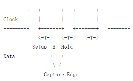
In this example:
T represents the clock cycle.
Setup is the setup time, indicating the time during which data must be stable before the capture edge.
Hold is the hold time, indicating the time during which data must be stable after the capture edge.
Capture Edge is the clock edge at which data is captured.
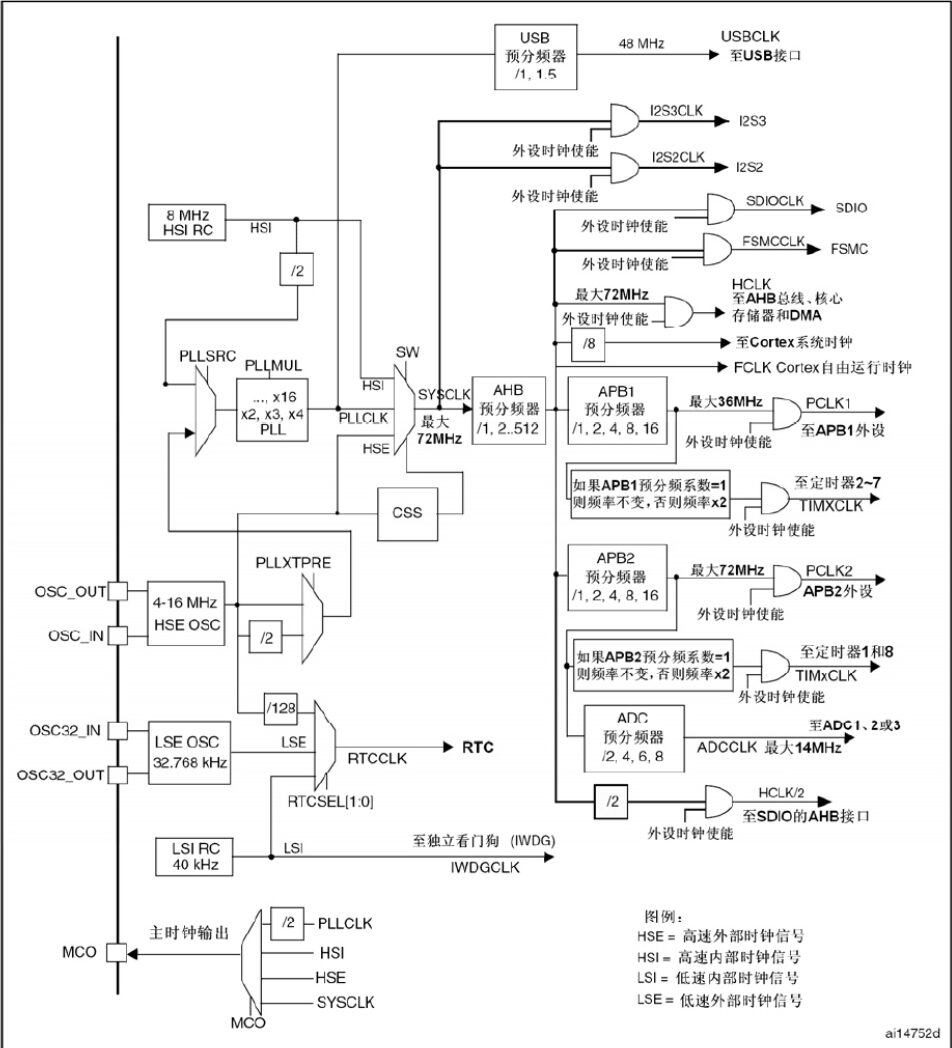
Additionally, here is a clock tree diagram for F103:
3. External Clock Circuit Design
First, let’s look at the circuit diagram:
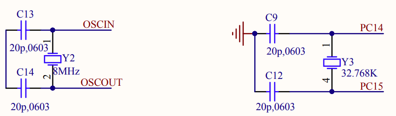
The circuit is divided into two parts: “High-Speed Clock, Low-Speed Clock”
Why use two clocks? One fast and one slow, won’t that interfere with the synchronization mentioned above?
First, let’s discuss why two clocks are used:
Microcontroller Units (MCUs) typically require clock sources at different rates to meet different system requirements. These requirements include processing capability, power consumption control, and peripheral clock demands. Here are some reasons for using high-speed and low-speed clocks:
High-Speed Clock
1. Performance Improvement:
The high-speed clock allows the MCU to operate at a faster frequency, thus improving processing speed and response time, which is crucial for applications that require rapid processing of large amounts of data or must respond quickly to external events.
2. Peripheral Support:
Some peripherals, such as USB interfaces, Ethernet controllers, or high-speed ADCs (Analog-to-Digital Converters), may require high-speed clocks to ensure they can operate at sufficient rates.
3. Data Throughput:
High-speed clocks can provide higher data throughput, which is essential for data-intensive tasks such as image processing or data acquisition.
Low-Speed Clock
1. Energy Saving:
The low-speed clock allows the MCU to run at lower frequencies, significantly reducing power consumption. This is very important for battery-powered devices, such as wearable devices or remote sensors, which need to maximize battery life.
2. Noise Reduction:
Operating at low-speed clocks can reduce electromagnetic interference (EMI) and signal noise, which is beneficial for applications requiring high-precision analog readings.
3. Peripheral Demand:
Some peripherals, such as real-time clocks (RTC) or low-speed serial communication interfaces (like I2C, SPI, etc.), can operate normally without high-speed clocks. Using low-speed clocks not only saves energy but also simplifies the overall system.
4. Dynamic Performance Adjustment:
Dynamic clock management can adjust the clock frequency based on the MCU’s workload, allowing for lower clock frequencies during light tasks and higher frequencies during high-performance needs.
How do different clocks avoid interference with each other?
For example, if the CPU needs to obtain time data from the RTC, this data must be safely transmitted from the low-speed clock domain to the high-speed clock domain. This is achieved by setting up synchronizers on the data lines, typically two or three stages of D flip-flops, ensuring signal stability and preventing metastability. When the microcontroller needs to switch between two clocks (for instance, switching from high-power mode to low-power mode), the internal clock management logic will switch during data transmission pauses to prevent data corruption during the transition.
Circuit Analysis
At first glance, this circuit seems quite simple, consisting of a crystal oscillator and two capacitors connected in series.
But why do we need two capacitors, and why are they connected this way?
(In the following text, C2 and C3 refer to the capacitors at both ends of the crystal oscillator.)
The crystal oscillator can be electrically equivalent to a parallel circuit of R1C1 (dynamic resistance R1 and capacitor C1) in parallel with a series capacitor C0, forming a network with two resonance points, where the lower frequency is series resonance and the higher frequency is parallel resonance.
Series Resonance: At the series resonance frequency, the impedance of the crystal oscillator is minimized, and the inductance L in the equivalent circuit of the crystal oscillator resonates with the internal capacitor C1.
Parallel Resonance: At the parallel resonance frequency, the impedance of the crystal oscillator is maximized, and the inductance L in the circuit resonates with the external parallel capacitor (such as C9 and C12 in the above circuit).
Within this narrow frequency range, the crystal oscillator is equivalent to an inductor L, combined with the external parallel capacitors (usually two capacitors C2 and C3), forming a parallel LC resonant circuit. This parallel resonant circuit can be used to build an oscillator, as it resonates at a specific frequency (the working frequency of the crystal oscillator).
By placing the crystal oscillator in a negative feedback circuit, a sine wave oscillator can be constructed. Negative feedback helps maintain the stability of the circuit, and the frequency stability of the crystal oscillator is very high; even if the parameters of other circuit components change, the frequency of the oscillator will not vary significantly.
In practical circuits, the two ends of the crystal oscillator are usually connected to capacitors C2 and C3. The total capacitance of these two capacitors in series equals the load capacitance required by the crystal oscillator (the specified capacitance value needed for the oscillator to work). Typically, one end of C2 and C3 connects to the crystal oscillator, and the other end connects to ground.
By selecting capacitors C2 and C3 equal to the load capacitance value of the crystal oscillator, the crystal circuit can achieve the specified nominal resonant frequency. This is because the external capacitance, together with the internal capacitor C1 of the crystal oscillator, determines the oscillation frequency.
Capacitance Calculation
Ce=2×CL−(Cs+Ci)
Where:
(Ce) is the value of each external capacitor connected at both ends of the crystal oscillator.
(CL) is the capacitive load value given in the crystal oscillator’s datasheet.
(Cs) is the lead capacitance, which can be obtained by consulting the chip’s datasheet.
(Ci) is the pin capacitance, which can also be obtained from the chip’s datasheet, typically between 3-6pF.