This article summarizes the learning process of STM32 and GD32, and I hope it serves as a reference for you.
1. Characteristics of SPI Communication
SPI is a full-duplex, synchronous, serial communication protocol.
- Full-duplex: Simultaneous data transmission and reception (Half-duplex transmits and receives data in a time-shared manner)
- Synchronous: All tasks must be completed before ending (Asynchronous allows multiple tasks to be completed simultaneously without waiting for others to finish)
- Serial: For one byte of data, it is transmitted in eight steps from the least significant bit to the most significant bit (For asynchronous, the same byte can be transmitted simultaneously over multiple data lines)
2. SPI Protocol
1. SPI Physical Layer (responsible for the physical transmission of data)
The SPI interface adopts a master-slave architecture: it supports one master to one slave and one master to multiple slaves, but does not support multiple masters.
STM32 and GD32 are consistent at the SPI physical layer
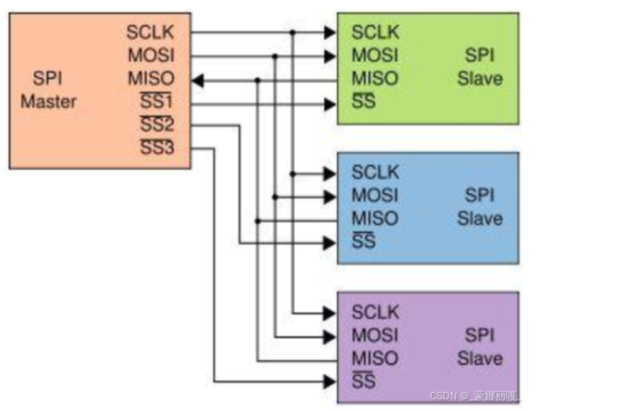
- SCK/SCLK: Clock signal generated and controlled by the master
- MOSI: Master Output Slave Input, data output from the master to the slave
- MISO: Master Input Slave Output, data input to the master from the slave
- SS/NSS: Slave Select Enable signal for master SPI communication
2. SPI Protocol Layer (responsible for the rules and standards of data transmission)
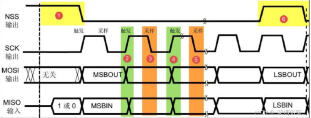
The SPI protocol defines the start and stop signals for communication, data validity, and clock synchronization.
-
Start and stop signals: NSS/SS goes low to start, goes high to end; in addition, pulling low selects which slave to communicate with.
-
Data validity: After NSS goes low, data on MISO and MOSI is prepared on the rising edge of SCK, and read on the falling edge of SCK. When NSS is high, data on MISO and MOSI is invalid.
-
Clock synchronization: The SCK clock signal must be strictly synchronized.
Sampling in STM32
(Odd/Even Edge Sampling Configuration)
CPHA=0, samples on odd edges
CPHA=1, samples on even edges
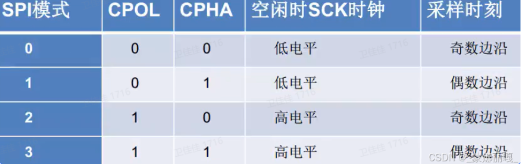
Sampling in GD32
CKPH=0, samples on odd edges
CKPH=1, samples on even edges
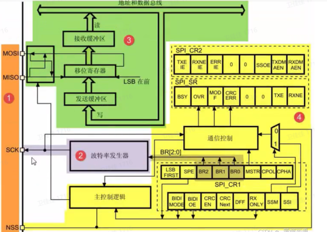
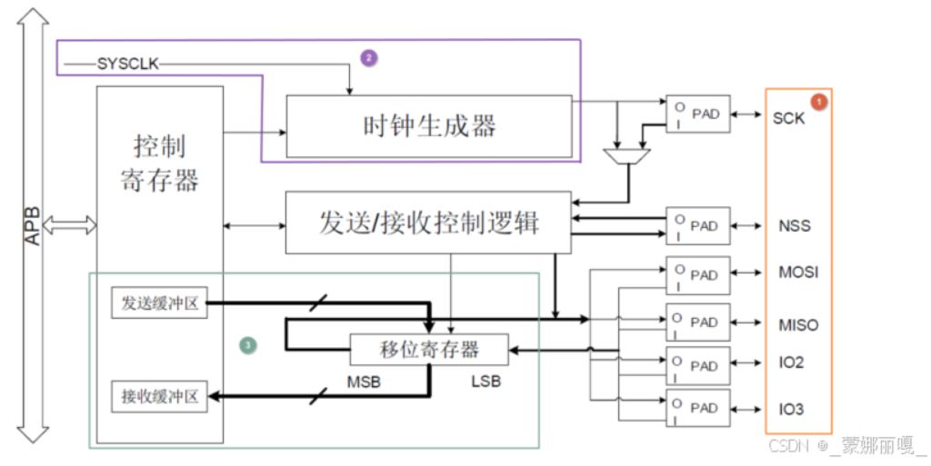
3. SPI Structural Block Diagram
It is important to note that the structures differ; STM32 allows selection of baud rate/bit rate.
STM32 Peripheral Structure:
GD32 Structure:
4. Usage Precautions
(1) Before switching the SPI clock, disable SPI; enable it again after the switch is complete.
(2) When sending data using SPI, setting the TBE flag does not indicate that the data transmission is complete; it only indicates that the data has moved from the transmit data register to the transmit shift register. If the CS pin is pulled high based on the TBE flag, due to the high execution efficiency of GD32 series MCUs, when the transmission rate is low, it may happen that when TBE is set, the CS pin is pulled high, while the data has not yet been fully sent, causing the slave to receive incorrect data. You can check the non-empty RBNE and TRANS flags in the receive data register to determine if the data transmission is complete before pulling the CS pin high.
(3) The MISO pin of SPI must be configured as a floating input mode; otherwise, data reception may be abnormal.
5. Software Configuration
Configuration Steps:
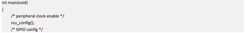
1. Configure Clock
STM32: RCC_APBxPeriphClockCmd
GD32: RCU_periph_clock_enable
2. GPIO Pin Configuration
STM32:
#define FLASH_SPIx SPI1#define FLASH_SPI_APBxClock_FUN RCC_APB2PeriphClockCmd#define FLASH_SPI_CLK RCC_APB2Periph_SPI1//CS(NSS) #define FLASH_SPI_CS_APBxClock_FUN RCC_APB2PeriphClockCmd#define FLASH_SPI_CS_CLK RCC_APB2Periph_GPIOB#define FLASH_SPI_CS_PORT GPIOB#define FLASH_SPI_CS_PIN GPIO_Pin_6//SCK #define FLASH_SPI_SCK_APBxClock_FUN RCC_APB2PeriphClockCmd#define FLASH_SPI_SCK_CLK RCC_APB2Periph_GPIOA#define FLASH_SPI_SCK_PORT GPIOA#define FLASH_SPI_SCK_PIN GPIO_Pin_5//MOSI #define FLASH_SPI_MOSI_APBxClock_FUN RCC_APB2PeriphClockCmd#define FLASH_SPI_MOSI_CLK RCC_APB2Periph_GPIOA#define FLASH_SPI_MOSI_PORT GPIOA#define FLASH_SPI_MOSI_PIN GPIO_Pin_7#define FLASH_SPI_CS_LOW() GPIO_ResetBits( FLASH_SPI_CS_PORT, FLASH_SPI_CS_PIN )#define FLASH_SPI_CS_HIGH() GPIO_SetBits( FLASH_SPI_CS_PORT, FLASH_SPI_CS_PIN )#define Dummy_Byte 0xFFvoid SPI_FLASH_Init(void){ SPI_InitTypeDef SPI_InitStructure; GPIO_InitTypeDef GPIO_InitStructure; FLASH_SPI_APBxClock_FUN ( FLASH_SPI_CLK, ENABLE ); FLASH_SPI_CS_APBxClock_FUN ( FLASH_SPI_CS_CLK|FLASH_SPI_SCK_CLK|FLASH_SPI_MOSI_PIN, ENABLE ); GPIO_InitStructure.GPIO_Pin = FLASH_SPI_CS_PIN; GPIO_InitStructure.GPIO_Speed = GPIO_Speed_50MHz; GPIO_InitStructure.GPIO_Mode = GPIO_Mode_Out_PP; GPIO_Init(FLASH_SPI_CS_PORT, &GPIO_InitStructure); /* SCK */ GPIO_InitStructure.GPIO_Pin = FLASH_SPI_SCK_PIN; GPIO_InitStructure.GPIO_Mode = GPIO_Mode_AF_PP; GPIO_Init(FLASH_SPI_SCK_PORT, &GPIO_InitStructure); /* MISO */// GPIO_InitStructure.GPIO_Pin = FLASH_SPI_MISO_PIN;// GPIO_Init(FLASH_SPI_MISO_PORT, &GPIO_InitStructure); /* MOSI */ GPIO_InitStructure.GPIO_Pin = FLASH_SPI_MOSI_PIN; GPIO_InitStructure.GPIO_Mode = GPIO_Mode_AF_PP; GPIO_Init(FLASH_SPI_MOSI_PORT, &GPIO_InitStructure); /*CS */ FLASH_SPI_CS_HIGH();GD32:
void gpio_config(void){#if defined GD32F10X_HD || GD32F30X_HD || GD32F20X_CL || GD32E10X/* SPI0 GPIO config:SCK/PA5, MISO/PA6, MOSI/PA7 */gpio_init(GPIOA, GPIO_MODE_AF_PP, GPIO_OSPEED_50MHZ, GPIO_PIN_5 | GPIO_PIN_7);gpio_init(GPIOA, GPIO_MODE_IN_FLOATING, GPIO_OSPEED_50MHZ, GPIO_PIN_6);/* PA3 as NSS */gpio_init(GPIOA, GPIO_MODE_OUT_PP, GPIO_OSPEED_50MHZ, GPIO_PIN_3);#elif defined GD32F1X0 || GD32F4XX || GD32F3X0 || GD32E23X#if defined GD32F1X0 || GD32F3X0 || GD32E23X/* SPI0 GPIO config: SCK/PA5, MISO/PA6, MOSI/PA7 */gpio_af_set(GPIOA, GPIO_AF_0, GPIO_PIN_5 | GPIO_PIN_6 | GPIO_PIN_7);#elif defined GD32F4XXgpio_af_set(GPIOA, GPIO_AF_5, GPIO_PIN_5 | GPIO_PIN_6 | GPIO_PIN_7);#endifgpio_mode_set(GPIOA, GPIO_MODE_AF, GPIO_PUPD_NONE, GPIO_PIN_5 | GPIO_PIN_6 | GPIO_PIN_7);gpio_output_options_set(GPIOA, GPIO_OTYPE_PP, GPIO_OSPEED_50MHZ, GPIO_PIN_5 | GPIO_PIN_6 | GPIO_PIN_7);gpio_mode_set(GPIOA, GPIO_MODE_OUTPUT, GPIO_PUPD_NONE, GPIO_PIN_3);gpio_output_options_set(GPIOA, GPIO_OTYPE_PP, GPIO_OSPEED_50MHZ, GPIO_PIN_3);#endifSET_SPI0_NSS_HIGH}3. SPI Peripheral Configuration
STM32:
SPI_InitStructure.SPI_Direction = SPI_Direction_1Line_Tx;SPI_InitStructure.SPI_Mode = SPI_Mode_Master;SPI_InitStructure.SPI_DataSize = SPI_DataSize_8b;SPI_InitStructure.SPI_CPOL = SPI_CPOL_High;SPI_InitStructure.SPI_CPHA = SPI_CPHA_2Edge;SPI_InitStructure.SPI_NSS = SPI_NSS_Soft;SPI_InitStructure.SPI_BaudRatePrescaler = SPI_BaudRatePrescaler_2;SPI_InitStructure.SPI_FirstBit = SPI_FirstBit_MSB;SPI_InitStructure.SPI_CRCPolynomial = 7;SPI_Init(FLASH_SPIx, &SPI_InitStructure);/* SPI */SPI_Cmd(FLASH_SPIx, ENABLE);GD32:
<!--br{mso-data-placement:same-cell;}table{mso-displayed-decimal-separator:"\.";mso-displayed-thousand-separator:"\, ";}tr{mso-height-source:auto;mso-ruby-visibility:none;}td{border:.5pt solid windowtext;}.NormalTable{cellspacing:0;cellpadding:10;border-collapse:collapse;mso-table-layout-alt:fixed;border:none; mso-border-alt:solid windowtext .75pt;mso-padding-alt:0cm 5.4pt 0cm 5.4pt; mso-border-insideh:.75pt solid windowtext;mso-border-insidev:.75pt solid windowtext}.fontstyle0{ font-family:Calibri; font-size:8pt; font-style:normal; font-weight:normal; color:rgb(0,0,0);}.fontstyle1{ font-size:12pt; font-style:normal; font-weight:normal; color:rgb(0,0,0);}-->void spi_config(void) {#if defined GD32E23XGD32F10X_HD|| GD32F30X_HD || GD32F1X0 || GD32F20X_CL || GD32F4XX || GD32F3X0 || GD32E10X || spi_parameter_struct spi_init_struct; /* SPI0 parameter config */spi_init_struct.trans_mode = SPI_TRANSMODE_FULLDUPLEX;spi_init_struct.device_mode = SPI_MASTER;spi_init_struct.frame_size = SPI_FRAMESIZE_8BIT;spi_init_struct.clock_polarity_phase = SPI_CK_PL_LOW_PH_1EDGE;spi_init_struct.nss = SPI_NSS_SOFT;spi_init_struct.prescale = SPI_PSC_256;spi_init_struct.endian = SPI_ENDIAN_MSB;spi_init(SPI0, &spi_init_struct); spi_enable(SPI0);#endif }4. Main Function Reference
This is my personal compilation; if there are any additions or questions, please point them out.