With the development of the technological era, Internet of Things (IoT) devices are rapidly developing across various industries, driving industrial upgrades and the arrival of the intelligent era. However, their security is particularly important, raising requirements for security research and improving protection. IoT security involves many aspects, and below we will share firmware extraction technology – solving the problem of not being able to correctly obtain data in U-Boot mode.
Note:This article is based on experiments conducted on my own development board to extract NAND Flash data. The methods introduced may not be universally applicable and are for reference only. Please forgive any shortcomings!
AThe NAND FLASH chip has read protection, making it impossible to correctly extract data from the chip using conventional operations such as JTAG/SWD.
Solution:
Please refer to the article:
Bypassing Read Protection Technology – Firmware Extraction from a Shared Bike Bluetooth Lock
Website link:
https://mp.weixin.qq.com/s/U83j3rzJwSp-3d6sDtgU1w
BThe extracted root filesystem is encrypted, and tools like Binwalk cannot parse it.
Encrypting the filesystem protects code security and increases the difficulty of extracting and analyzing firmware. This method is increasingly adopted by manufacturers. However, from a security perspective, it is necessary to correctly decrypt the firmware, obtain the filesystem, and then conduct vulnerability mining.
Solution:
First, extract the BootLoader partition data and kernel partition data from the NAND FLASH, then perform reverse analysis to identify the decryption program.
ABootLoader
In simple terms, the BootLoader is a small piece of code that starts executing when the system powers on, initializes hardware devices, prepares the software environment, and finally calls the operating system kernel.
The BootLoader runs first, copying the kernel file from the NAND FLASH to memory, and passing the configured parameters to the kernel to run it.
The BootLoader decompresses the compressed files on FLASH before running them. (Specifically decrypting the kernel and filesystem stored in FLASH is crucial for later firmware cracking).
BLinux Kernel
Parsing the startup parameters passed by U-Boot
Mounting the root filesystem
Starting the first application
CFilesystem
Includes the root filesystem and the filesystem built on the Flash memory device. It contains the applications, libraries, and other components necessary for the Linux system to operate.(The applications in the system are the targets for vulnerability analysis and mining.)
DCommon Commands
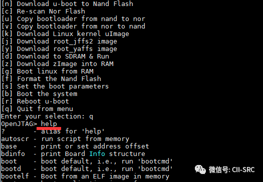
mtdpart: View partitions
md: Display memory contents
md command usage: md start_address length (addresses and lengths are generally in hexadecimal format)
nand read: Read data from NAND Flash to memory
nand read[.jffs2] addr off size: Read size bytes of data from the NAND Flash starting at offset addr into memory.
nand bad: View bad blocks in NAND Flash
ENAND Flash Introduction: K9F2G08U0A Model
i. NAND Flash Address Mechanism (Very Important):
1. The storage unit of NAND Flash is composed of Blocks, which are made up of Pages, and data is stored on Pages.
2. NAND Flash reads and writes data on a page (Page) basis.
3. See the K9F2G08U0A datasheet for information on address cycles:
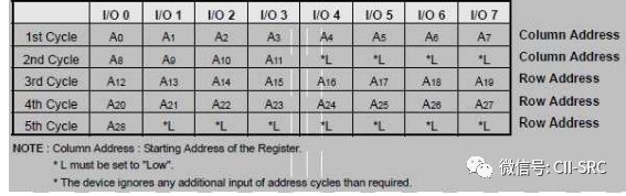
From the above image, it can be seen that K9F2G08U0A is implemented using 5 cycles. Since NAND Flash reads data on a page basis and erases data on a block basis, there are three types of addresses:
-
Column Address: Column address, the low 8 bits of the address, i.e., the offset address within the page.
-
Page Address: Page address.
-
Block Address: Block address.
Taking address 0xBB8CCB8 as an example, the address transfer process requires five address cycles:
0xBB8CCB8 = 00001011 1011 1000 1100 1100 1011 1000
-
First cycle: A[0:7] which is B8
-
Second cycle: A[8:11] takes four bits 1100, then adds 4 bits 0, which is 0000 1100, i.e., 0C
-
Third cycle: A[12:19] takes eight bits 1000 1100, i.e., 8C
-
Fourth cycle: A[20:27] takes eight bits 1011 1011, i.e., BB
-
Fifth cycle: A[28] takes one bit 0, filling to eight bits, which is 0000 0000, i.e., 00
Analyzing back, NAND Flash receives the first two cycles of address A[0:11], which is 0CB8, i.e., 1100 1011 1000. Analysis: A[10:0]=100 1011 1000=1208, indicating the 1208th Byte.
ii. NAND Flash Read Commands
1. Refer to the K9F2G08U0A manual.
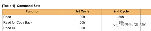
2. Based on the K9F2G08U0A address cycle and Read command, write the following code to read NAND Flash data:
void nand_select(void){ /* Enable chip select */ NFCONT &= ~(1 << 1);}void nand_deselect(void){ /* Disable chip select */ NFCONT |= (1 << 1);}void nand_cmd(unsigned char cmd){ volatile int i; NFCCMD = cmd; for(i=0; i < 10; i++);}void nand_addr_byte(unsigned char addr){ volatile int i; NFADDR = addr; for(i=0; i < 10; i++);}unsigned char nand_data(void){ return NFDATA;}void wait_ready(void){ while (!(NFSTAT & 1));}void nand_read(unsigned int addr, unsigned char *buf, unsigned int len){ int i = 0; int page = addr / 2048; int col = addr & (2048 - 1); nand_select();// Select chip while (i < len){ /* Send 00h command */ nand_cmd(00); /* Send address */ /* col addr */ nand_addr_byte(col & 0xff); nand_addr_byte((col >> 8) & 0xff); /* row/page addr */ nand_addr_byte(page & 0xff); nand_addr_byte((page >> 8) & 0xff); nand_addr_byte((page >> 16) & 0xff); /* Send 30h command */ nand_cmd(0x30); /* Wait for ready */ wait_ready(); /* Read data */ for (; (col < 2048) && (i < len); col++){ buf[i++] = nand_data(); } if (i == len){ break; } col = 0; page++; } nand_deselect(); }AConventional Method – Extracting data through U-Boot mode
Enter U-Boot mode, use the nand read command to read the desired data into memory, then dump the memory.
BUnconventional Method – Directly sending commands to NAND Flash to read data
When reading data from NAND FLASH into memory, there is ECC verification to determine if the data is correct; if there are bad blocks in the data read, it will not be possible to successfully read the data into memory, making it impossible to extract data through U-Boot mode.
AConventional Method: Extracting Data through U-Boot Mode
i. Enter U-Boot mode and use help to view commands
During system startup, press spacebar to enter U-Boot mode
ii. Use mtdpart to view partitions
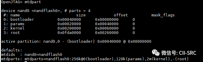
It can be seen that NAND Flash has four partitions, and the size of each partition can be calculated.
iii. Use the nand read command to read BootLoader partition data into memory
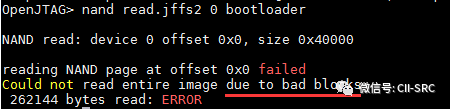
According to the prompt, it can be seen that the read failed due to the presence of bad blocks.
BBootLoader partition data has bad blocks, using an unconventional method to extract data
i. OpenOCD connects to the target device, opening port 4444
ii. Write the following script based on NAND Flash instructions and address cycle characteristics (5 cycles) to read data byte by byte:
#!/usr/bin/env rubyrequire 'net/telnet'# NFCONF __REG(0x4E000000) //NAND flash configuration # NFCONT __REG(0x4E000004) //NAND flash control # NFCCMD __REG_BYTE(0x4E000008) //NAND flash command # NFADDR __REG_BYTE(0x4E00000C) //NAND flash address # NFDATA __REG_BYTE(0x4E000010) //NAND flash datadebug = Net::Telnet::new("Host" => "localhost", "Port" => 4444)dumpfile = File.open("dump_bootloader.bin", "a+")debug.cmd("halt")debug.cmd("mww 0x4E000004 1")debug.cmd("mwb 0x4E000008 0x00") # Commanddebug.cmd("mwb 0x4E00000C 0x00") # 5 address cyclesdebug.cmd("mwb 0x4E00000C 0x00")debug.cmd("mwb 0x4E00000C 0x00")debug.cmd("mwb 0x4E00000C 0x00")debug.cmd("mwb 0x4E00000C 0x00")debug.cmd("mwb 0x4E000008 0x30") # Command$i = 0$num = 0x1000while $i < $num do response =debug.cmd("mdb 0x4E000010 1") # Read 1 byte value = response.match(/0x4e000010: ([0-9a-fA-F]{2})/)[1].hex dumpfile.write([value].pack("c")) $i +=1end;dumpfile.closedebug.closeiii. Compare the data obtained through the script with the data seen using nand dump 0
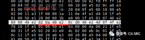
1. nand dump 0 data
2. Data read by the script dump_bootloader.bin
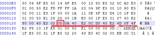
By comparison, it can be seen that at position 0x125, the data in dump_bootloader.bin has an extra byte 0D, thus the data read using the nand read command cannot pass verification.
In the presence of bad blocks, successfully obtaining BootLoader partition data indicates that the method of obtaining data through chip instruction operations is feasible.
AReading kernel partition data into memory at address 0
nand read.jffs2 0 kernel
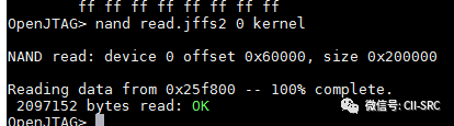
Using a script, dump kernel partition data from memory
#!/usr/bin/env rubyrequire 'net/telnet'debug = Net::Telnet::new("Host" => "localhost", "Port" => 4444)debug.cmd("halt")debug.cmd("dump_image dump_kernel_part.bin 0x0 0x200000")debug.closeView the read data
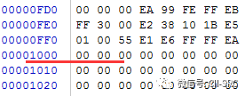
It can be seen that the data after 0x1000 is incorrect.
Reason:
This is because the on-chip memory is only 4k, so data exceeding 4k cannot be read into address 0.
Solution:
Read the kernel partition data into the flash SDRAM, starting at address 0x30000000 (refer to the manual).
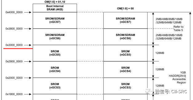
BReading kernel partition data into memory at the starting address of SDRAM
nand read.jffs2 0x30000000 kernel
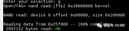
Using a script, dump kernel partition data from memory
require 'net/telnet'debug = Net::Telnet::new("Host" => "localhost", "Port" => 4444)debug.cmd("halt")debug.cmd("dump_image dump_kernel.bin 0x30000000 0x200000")debug.closeView the read data
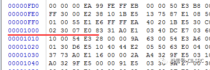
Correctly read data, method is feasible
Through practical operations, the problem of not being able to correctly extract NAND Flash partition data in U-Boot mode has been solved, and the feasibility of extracting NAND Flash partition data with bad blocks through chip instruction operations has been verified; the issue of incomplete extraction of kernel partition data larger than the on-chip memory size has also been properly addressed.
Successfully extracting BootLoader partition data and kernel partition data provides a basis for the next step of cracking the encrypted root filesystem.
Original source: Critical Infrastructure Security Emergency Response Center