The design of SOC’s SRAM, with waveform simulation verification using VCS + Verdi. SRAM serves as system cache, existing in the form of an AHB Slave. SRAM host features: supports 8-bit, 16-bit, and 32-bit read/write operations; single-cycle read/write; low power operation (the system can choose one or more SRAMs); supports DFT/BIST functionality.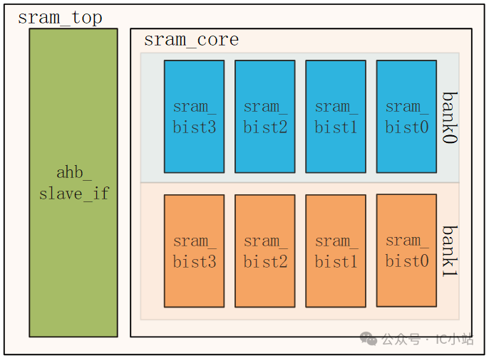 1. sramc_top is the top-level design of SRAM, which includes BIST and DFT functionality.
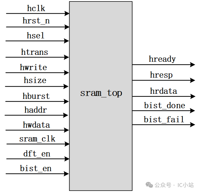 ● SRAM Control: Connects SRAM to the AHB bus, converting read/write operations on the AHB bus into standard SRAM read/write operations.● SRAM’s address and data are read/written in the same cycle. The AHB bus sends the address and control signals in the previous clock cycle, and the data in the next clock cycle, requiring a clock edge operation to align them in the same cycle.
|
hclk |
System clock |
|
hrst_n |
System reset |
|
hsel |
Slave select signal, active high, sent by the master The hsel signal must be used in conjunction with the hready signal to ensure the correctness of the transmission |
|
htrans |
AHB bus transfer type |
|
hwrite |
1 write transfer, 0 read transfer |
|
hsize |
Size of data for each transfer,hsize = 000:8bit,010:32bit,011:64bit The transfer size of hsize cannot exceed the bit width of hwdata |
|
hburst |
Transfer type, here using000 single data transfer |
|
haddr |
Data address |
|
hwdata |
Data to be written |
|
dft_en |
DFT mode enable signal |
|
bist_en |
BIST mode enable signal |
|
hready |
Handshake signal from the slave to the master, In the AHB2 protocol, only the hready signal is referred to, defaulting to1 |
|
hresp |
Slave response signal,00 : OKAY, 01 : ERROR, 10 : RETRY, 11 : SPLIT |
|
hrdata |
Data read out |
|
bist_done |
Test completion signal |
|
bist_fail |
[7:0], the working status of each bist. |
|
hresp Slave response (AHB bus signal) |
||
|
00 |
OKAY |
hready=1’b1,transfer complete;hready=1’b0,insert extra cycle |
|
01 |
ERROR |
Operation unsuccessful |
|
10 |
RETRY |
Indicates that the transfer is not complete, continue to retry until the transfer is complete |
|
11 |
SPLIT |
This transfer is not complete, re-execute the transfer operation the next time the bus is used |
|
hburst Transfer type (AHB bus signal) |
||
|
000 |
SINGLE |
Single data |
|
001 |
INCR |
Variable-length increment |
|
010 |
WRAP4 |
Wrap around 4 data |
|
011 |
INCR4 |
Increment 4 data |
|
100 |
WRAP8 |
Wrap around 8 data |
|
101 |
INCR8 |
Increment 8 data |
|
110 |
WRAP16 |
Wrap around 16 data |
|
111 |
INCR16 |
Increment 16 data |
This increment and wrap around refer to the address, incrementing means increasing with the previous address, and wrap around means the data transfers back within a boundary. This boundary is determined by hsize and hburst. Note that the boundary cannot exceed 1KB.
|
htrans Transfer type (AHB bus signal) |
||
|
00 |
IDLE |
Slave ignores the current transfer |
|
01 |
BUSY |
Indicates that the master is processing data, the slave needs to ignore the current transfer |
|
10 |
NONSEQ |
Indicates that this is a single data, or the first data of a Burst |
|
11 |
SEQ |
Remaining data of the Burst transfer |
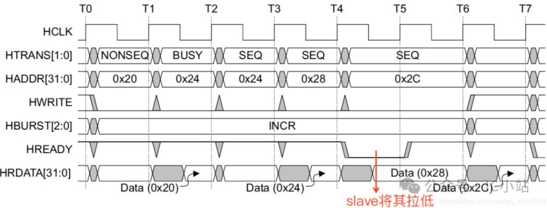
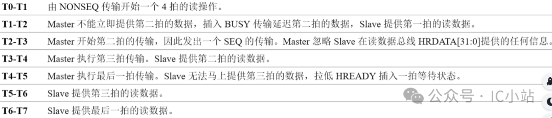 ● ahb_slave_if converts read/write operations on the AHB bus into standard SRAM read/write operations.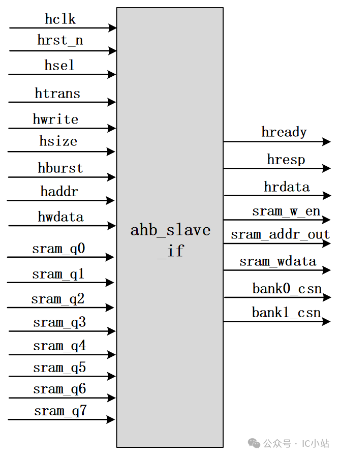
sram_w_en :SRAM read write signal.
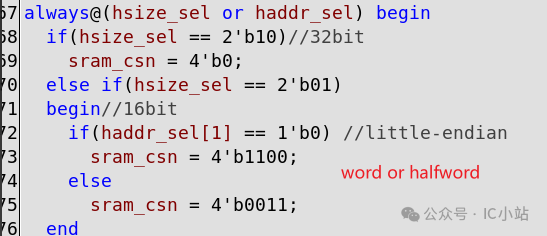
sram_csn : Selects the data read/write bit width through the chip select signal: byte, half word, word
|
hsize[1:0] |
haddr[1:0] |
sram_csn[3:0] |
|
10(word) |
XX |
0000 |
|
01(half word) |
0X |
1100 |
|
01(half word) |
1X |
0011 |
|
00(byte) |
00 |
1110 |
|
00(byte) |
01 |
1101 |
|
00(byte) |
10 |
1011 |
|
00(byte) |
11 |
0111 |
 ● sram_core integrates 8 SRAM blocks, with MBIST and DFT functionality.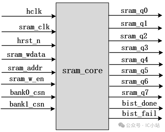
|
sram_clk |
sram_sp_hse_8kx8 Module’s working clock |
|
sram_wdata |
Data to be written |
|
sram_addr |
Data address |
|
sram_w_en |
Read/write enable |
|
bank0_csn |
Chip select sram3 – 0, from ahb_slave_if |
|
Bank1_csn |
Chip select sram7 – 4 |
|
sram_q7-0 |
Read out each block of data from SRAM |
|
bist_done |
Test completion signal |
|
bist_fail |
[7:0], the working status of each bist. |
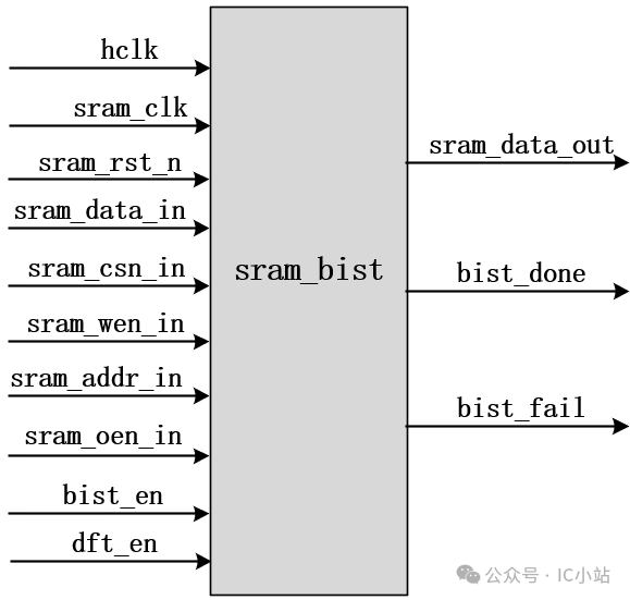
● sram_bist module implements DFT and BIST functionality
|
sram_data_in |
Data to be written |
|
sram_csn_in |
Chip select signal |
|
sram_wen_in |
Read/write enable signal,0 write,1 read |
|
sram_addr_in |
Data address |
|
sram_oen_in |
Set to0 to enable |
|
bist_en |
MBIST mode |
|
dft_en |
DFT mode |
|
sram_data_out |
DFT ternary operation determines whether it is DFT test data or data |
|
bist_done |
Test completion signal |
|
bist_fail |
Test failure signal |
● mbist_8kx8 block implements the “March” algorithm (for all 0s or all 1s), to detect the functionality of SRAM.
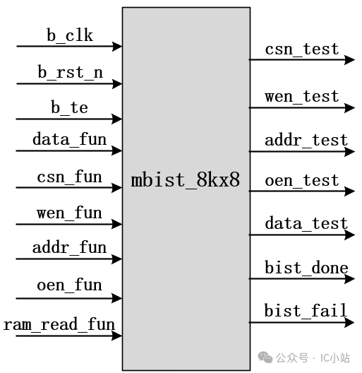
|
b_clk |
Clock signal |
|
b_rat_n |
Reset signal |
|
b_te |
Enable signal, whether to enable BIST mode |
|
data_fun |
Input data |
|
csn_fun |
Chip select signal |
|
wen_fun |
Read/write enable signal |
|
addr_fun |
Input data address |
|
oen_fun |
Set to0 to enable |
|
ram_read_fun |
sram_sp_hse_8kx8 module’s SRAM data, used here to determine bist_fail |
|
csn_test |
Chip select signal, determined by b_te whether to use test or data (ternary operation) |
|
wen_test |
Read/write signal, determined by b_te whether to use test or data (ternary operation) |
|
oen_test |
Set to0 to enable, determined by b_te whether to use test or data (ternary operation) |
|
addr_test |
Data address, determined by b_te whether to use test or data (ternary operation) |
|
data_test |
Input data, determined by b_te whether to use test or data (ternary operation) |
|
bist_done |
BIST test completion signal |
|
bist_fail |
Signal indicating whether SRAM functionality is erroneous |
mbist state transition (“March” algorithm: for all 0s or all 1s):
Initialization phase (IDEL1 → P1_WRITE0 → IDEL2)
First phase read/write test (IDEL2 → P2_→ IDEL3)
Second phase read/write test (IDEL3 → P3_→ IDEL4)
Third phase read/write test (IDEL4 → P4_→ IDEL5)
Fourth phase read/write test (IDEL5 → P5_→ IDEL6)
Final verification phase (IDEL6 → P6_ → IDEL1)
IDEL2、3、4、5、6 are prepared for the next phase,IDEL1 is the test completion, returning to the initial state
|
BIST test state machine |
|
|
write “0”(initial SRAM) |
test_address 0–>1fff |
|
read “0”——> compare ——–>write “1” |
test_address 1fff–>0 |
|
read “1”——> compare ——–>write “0” |
test_address 0–>1fff |
|
write “1”——> read “1”——–>compare |
test_address 1fff–>0 |
|
write “0”——> read “0”——–>compare |
test_address 0–>1fff |
|
write “1”——> read “1”——–>compare |
test_address 1fff–>0 |
|
write “0”——> read “0”——–>compare |
test_address 0–>1fff |
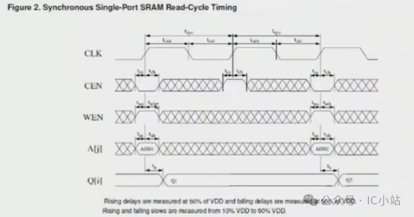
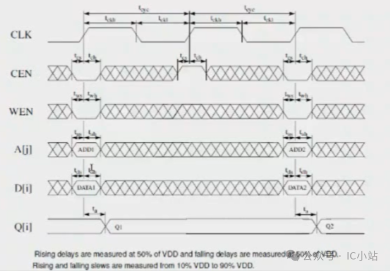
● SRAM memory array (sram_sp_hse_8kx8) is an IP generated by the memory compiler, SRAM power-down programs lose data, so there is no need to check the initial values upon power-up, and no reset signal is required. The address is 13 bits, with a depth of 8192.
oen is kept low.
wen is 0 for write, and 1 for read. Chip select signal cen is low: wen, address, and data are valid.SRAM working timing: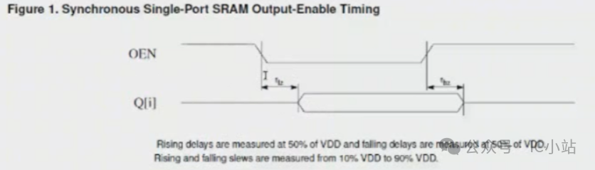
 The above is the design of the SRAM controller section. For specific code and documentation, please follow the public account and reply “ahb_sram” to obtain.