Chip Resource Introduction
The RK3588 has a total of 5 PCIe controllers, with the same hardware IP but different configurations. One of them is a 4-Lane DM mode that can be used as an EP, while another is a 2-Lane and 3 single-Lane controllers that can only be used as RC. The RK3588 has two types of PCIe PHY, one being pcie3.0 PHY, which includes 2 ports with a total of 4 lanes, and the other is a pcie2.0 PHY with 3 ports, each being 2.0 single-lane, used in conjunction with SATA and USB. The 4 lanes of the pcie3.0 PHY can be split according to actual needs, and after splitting, the corresponding controllers need to be configured properly. All configurations are completed in the DTS, and there is no need to modify the driver.
Usage Restrictions:
1. After splitting the pcie30phy, the pcie30x4 controller, when operating in 2-Lane mode, can only be fixed to work with pcie30phy’s port0; when operating in 1-Lane mode, it can only be fixed to work with pcie30phy’s port0lane0;
2. After splitting the pcie30phy, the pcie30x2 controller, when operating in 2-Lane mode, can only be fixed to work with pcie30phy’s port1; when operating in 1-Lane mode, it can only be fixed to work with pcie30phy’s port1lane0;
3. When the pcie30phy is split into 4 single-lanes, pcie3phy’s port0lane1 can only be fixed to work with pcie2x1l0 controller, and pcie3phy’s port1lane1 can only be fixed to work with pcie2x1l1 controller;
4. The pcie30x4 controller operating in EP mode can use 4-Lane mode, or in 2-Lane mode, use pcie30phy’s port0, while 2 lanes of pcie30phy’s port1 can be used as RC with other controllers. By default, when using a common clock as the reference clock, it is not possible to have pcie30phy port0’s lane0 operate in EP mode while lane1 operates in RC mode with other controllers, because both lanes of Port0 share the same input reference clock, and using the clock for both RC and EP may cause conflicts. 5. If only one port of RK3588 pcie30phy is used, the other port also needs to be powered, and signals like refclk can be grounded.
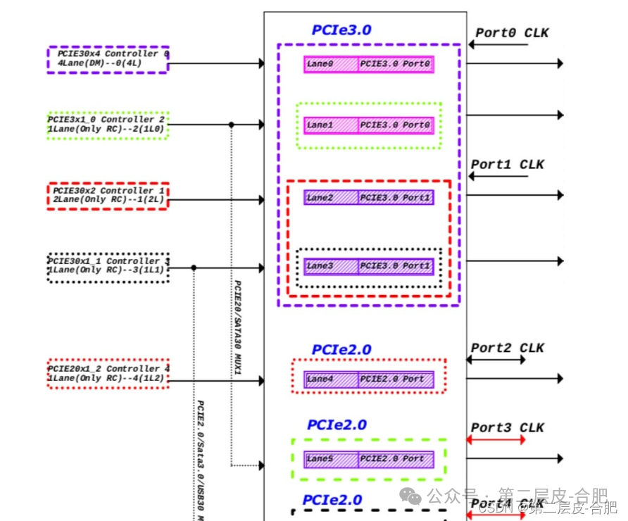
DTS Configuration
Configuration Key Points
The configuration of PCIe is mostly fixed, and there are not many variables that need to be configured in the board-level DTS. Refer to the following key points for configuration:
1. Controller/PHY Enable: After determining the solution, select the correct controller and PHY to enable based on the schematic. Note that the index of the controller and the index of the PHY do not necessarily match in order, such as RK3588’s pcie2x1l0 not corresponding to combphy0_ps;
2. Controller: Some controllers (like RK3588’s pcie2x1l0 and pcie2x1l1) have more than one PHY option, configure “phys” correctly according to the design;
3. Controller: As RC, it usually requires configuring “reset-gpios”, which corresponds to the schematic’s PCIe “PERSTn” signal;
4. Controller: As RC, it may require configuring “vpcie3v3-supply”, which corresponds to the fixed regulator controlled by the PCIe “PWREN” GPIO signal;
5. Controller: When used as EP, it is necessary to modify “compatible” to the corresponding string for EP mode;
6. PHY: The pcie30phy has a total of 4 lanes, which can be split for use, and needs to be configured correctly according to the solution for “rockchip,pcie30-phymode”;
DTS Property Description
1. compatible = <?>; Optional configuration item: This item sets whether the PCIe interface is used in RC mode or EP mode. For RK3568 as RC functionality, it needs to be configured as compatible = “rockchip,rk3568-pcie”, “snps,dw-pcie”; if it needs to be changed to EP mode, it should be modified to compatible = “rockchip,rk3568-pcie-ep”, “snps,dw-pcie”; similarly for RK1808 and RK3588, just replace the rk3568 field with rk1808 and rk3588 respectively.
2. reset-gpios = <&gpio3 13 GPIO_ACTIVE_HIGH>; Must configure item: This item sets the PCIe interface’s PERST# reset signal; whether for slot or soldered devices, please find this pin on the schematic and configure it correctly. Otherwise, it is very likely that the link establishment cannot be completed stably. It should also be noted that if multiple lanes of the PCIe interface are split, then each split node must be configured with a different PERST# signal line.
3. num-lanes=<4>; Optional configuration item: This configuration sets the number of lanes used by the PCIe device, which has been configured in the chip-level dtsi and does not need to be adjusted by default. When used with split PHY, it is recommended to configure according to the actual hardware.
4. max-link-speed=<2>; Optional configuration item: This configuration sets the bandwidth version of PCIe, where 1 indicates Gen1, 2 indicates Gen2, and 3 indicates Gen3. It should be noted that this configuration is chip-related and generally does not need to be configured for each board, so we have configured it in the chip-level dtsi, and it is merely a testing measure or a downgrade measure after customer board design anomalies.
5. status=<okay>; Must configure item: This configuration needs to enable both the PCIe controller node and the corresponding PHY node simultaneously. 6. vpcie3v3-supply=<&vdd_pcie3v3>; Optional configuration item: Used to configure the 3V3 power supply for PCIe peripherals (in principle, our hardware reference schematic combines the 12V power supply and 3V3 power supply control for the PCIe slot, so after configuring the 3V3 power supply, the 12V power supply is controlled together). If the board-level 3V3 for PCIe peripherals needs to be controlled, then define a corresponding regulator as shown in the example, and refer to Documentation/devicetree/bindings/regulator/ for regulator configuration. It should also be noted that if it is a PCIe3.0 controller, an external 100M crystal oscillator chip is generally required, and the power supply for this crystal oscillator chip should, in principle, be shared with the 3V3 of the PCIe peripherals. Therefore, after configuring this item, in addition to confirming the 3V3 power supply for the peripherals, it is also necessary to confirm whether the clock output of the external crystal oscillator chip is normal. Generally, the external crystal oscillator chip requires a stable period to output the clock. Therefore, please strictly refer to the minimum value specified in the clock chip’s manual and specify the value of the startup-delay-us attribute in the power node with a testing margin. Additionally, for hardware designs that discharge slowly after power off, specify the value of the off-on-delay-us attribute in the power node to ensure sufficient power cycling operations. For example, for rk3568, detailed examples can be referenced in the vcc3v3_pcie node of the rk3568-evb1-ddr4-v10.dtsi file.
7. phys optional configuration item: Used to configure the phandle reference of the PHY used by the controller, some controllers can route to multiple PHYs (like RK3588’s pcie2x1l0 and pcie2x1l1), and it should be noted that different PHY reference methods may vary, comboPHY needs to specify the working mode of the PHY simultaneously;
8. rockchip,bifurcation; optional configuration item: This is a configuration unique to the RK3568 chip. It can split the pcie3x2’s 2 lanes into two single-lane controllers for use. The specific configuration method is to enable both the pcie3x1 and pcie3x2 controller nodes and pcie30phy in the dts, and add the rockchip,bifurcation attribute in both pcie3x2 and pcie3x1 nodes. Refer to rk3568-evb6-ddr3-v10.dtsi. Otherwise, by default, the pcie3x1 controller cannot be used. At this time, lane0 is used by the pcie3x2 controller, and lane1 is used by the pcie3x1 controller, strictly following our schematic in the hardware layout. Also note that in this mode, both single-lane controllers must operate in RC mode simultaneously. Additionally, it should be particularly noted that when PCIe 3.0 is split into 2 single lanes connected to two different peripherals, since the crystal oscillator and its power supply are controlled by the same route. At this time, do not configure the vpcie3v3-supply to one of the controllers, otherwise, it will cause the controller that has obtained the 3V3 voltage operation permission to interfere with the normal initialization of the peripherals connected to the other controller. At this time, the regulator corresponding to vpcie3v3-supply should be configured as regulatorboot-on and regulator-always-on.
9. prsnt-gpios=<&gpio415 GPIO_ACTIVE_LOW>; Optional configuration item: Used to drive recognition of whether peripherals exist and related peripheral circuits. If a valid level is detected, skip the device detection process. According to the PCIe electrical characteristics protocol document, this GPIO indicates that there is a device connected when at a low level. If the board design is opposite to this, it can be modified to GPIO_ACTIVE_HIGH to indicate that a high level means a device is connected.
10. rockchip,perst-inactive-ms=<500>; Optional configuration item: Used to configure the reset time of the device #PERST reset signal, in milliseconds. According to the PCIe Express Card Electromechanical Spec requirements, the minimum requirement for downstream device power stability before releasing #PERST is 100ms. If this item is not configured, the RK driver defaults to 200ms. If it still does not meet the peripheral working requirements, it can be adjusted as appropriate based on actual measurements.
11. supports-clkreq; Optional configuration item: Valid only in RC mode, please confirm that the CLKREQ# pinctrl iomux has been configured as function io. If this attribute exists, it indicates the existence of the CLKREQ# signal routing from the root port to the downstream device, and the host bridge driver can program based on the existence of the CLKREQ# signal. For example, if there is no CLKREQ# signal, the root port will be set to not support PM L1 Substates.
12. rockchip,lpbk-master special debugging configuration: This configuration is for loopback signal testing, using the PCIe controller to construct a simulated loopback master environment, allowing the device under test to enter the slave model. Please do not configure this for non-simulated verification laboratory RX loop requirements. Also note that Gen3 controllers may need to configure compliance mode to enter loopback slave mode. If the reader does not understand what loopback testing is, it indicates that this is not the configuration you are looking for, please do not ask questions regarding this configuration. 13. rockchip,compliance-mode special debugging configuration: This configuration is for compliance signal testing, using the PCIe controller to force entry into compliance test mode. The default TX test should use a test SMA fixture to enter compliance, and does not need to be forced. This configuration is reserved for testing Gen3 mode loopback slave, as laboratory tests may require Gen3 loopback testing to enter compliance mode. If the reader does not understand what compliance testing is, it indicates that this is not the configuration you are looking for, please do not ask questions regarding this configuration.