
Abstract: By researching the factors such as different line widths, different dielectric thicknesses, variations in dielectric constant, layer browning, and line compensation, this study analyzes the main factors affecting PCB impedance and the varying degrees of impedance influence, providing the best recommendations for high precision impedance design of PCBs.
0
Introduction
In the integrated application of ICs (Integrated Circuits), once the signal transmission frequency (emission) of the assembled PCBA (Printed Circuit Board Assembly) reaches a certain value, it will be affected by the PCB traces themselves, leading to severe distortion or complete loss of the transmitted signal. This indicates that what flows through the highly integrated PCB traces is not current, but rather the transmission of square wave signals or pulses in terms of energy, and the resistance encountered during this signal transmission is referred to as “impedance.” Especially in the context of the rapid promotion and application of high-frequency and high-speed signal technologies in the electronic communication industry, customer requirements for PCBs are not just about meeting physical performance; the demands for electrical performance are increasingly stringent, such as 7% and 5% impedance tolerances, insertion loss control, and so forth. The PCB manufacturing industry faces challenges not only in processing capabilities but also in design capabilities. It is evident that impedance is becoming increasingly important in PCB applications with high integration.
1
Experimental Method
 1.1 Equipment and Materials
Equipment: CITS900S4 Polar Impedance Tester; TEKTRONIX Impedance Tester.
Materials: Semi-cured sheets with specifications of 1080, 2313, 2116, 7628; 0.10 mm inner layer core board.
1.2 Test Items
(1) The impact of different line widths on single line impedance and differential impedance;
(2) The impact of different dielectric thicknesses on single line impedance and differential impedance;
(3) The impact of different εr (dielectric constant) variations on single line impedance and differential impedance;
(4) The impact of dielectric thickness control on the residual copper rate of impedance strips and internal impedance control areas;
(5) The impact of line layer browning (or blackening) on impedance values;
(6) The impact of line compensation on impedance.

2
Results and Discussion
2.1 The Impact of Line Width Variation on Single Line Impedance and Differential Impedance
Line width control is an important factor affecting the precision of PCB impedance control. The impact of different semi-cured sheets and impedance line widths on impedance is listed in Tables 1 and 2.
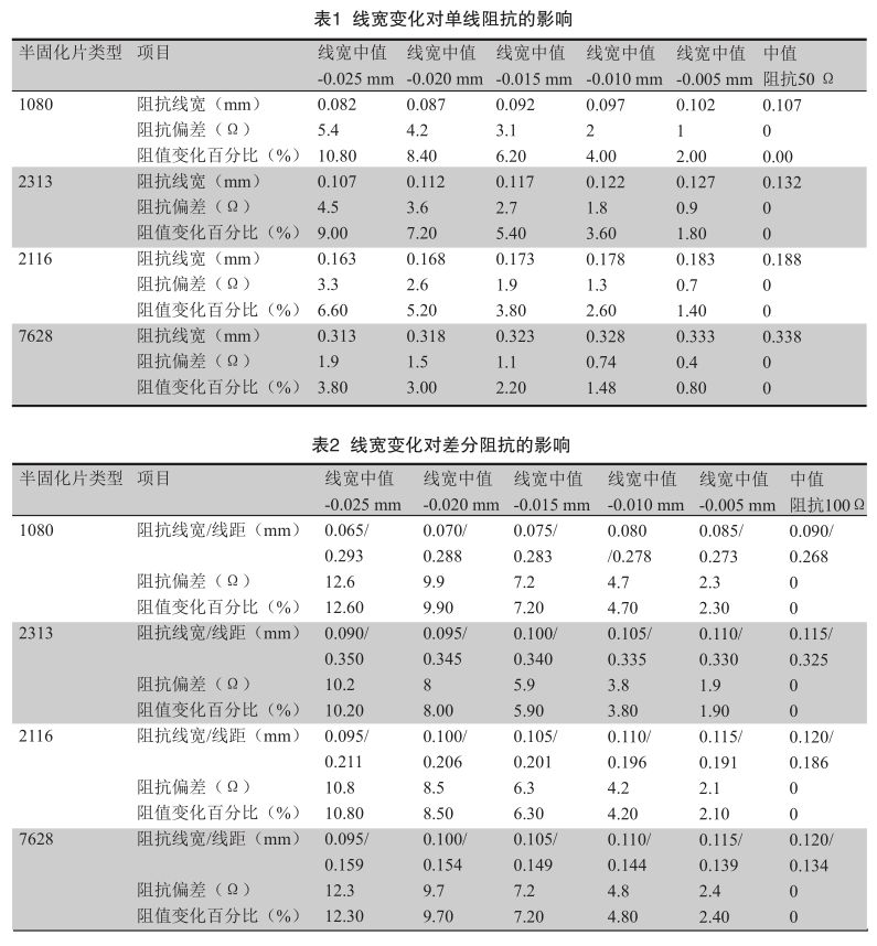
The thicker the semi-cured thickness, the smaller the impact of line width variation on the impedance value. The thinner the semi-cured thickness, the greater the impact of line width variation on the impedance value. Particularly, if a single sheet of 1080 or thinner semi-cured sheet is used as the dielectric layer for the impedance line, special attention must be paid to controlling the fluctuation range of the impedance line width.
2.2 The Impact of Dielectric Thickness on Single Line Impedance and Differential Impedance
Dielectric thickness has a significant impact on impedance accuracy, including the dielectric layer thickness of the core board and the thickness after pressing the semi-cured sheet. The impact of different semi-cured sheets and dielectric thicknesses on impedance is analyzed, as shown in Tables 3 and 4.
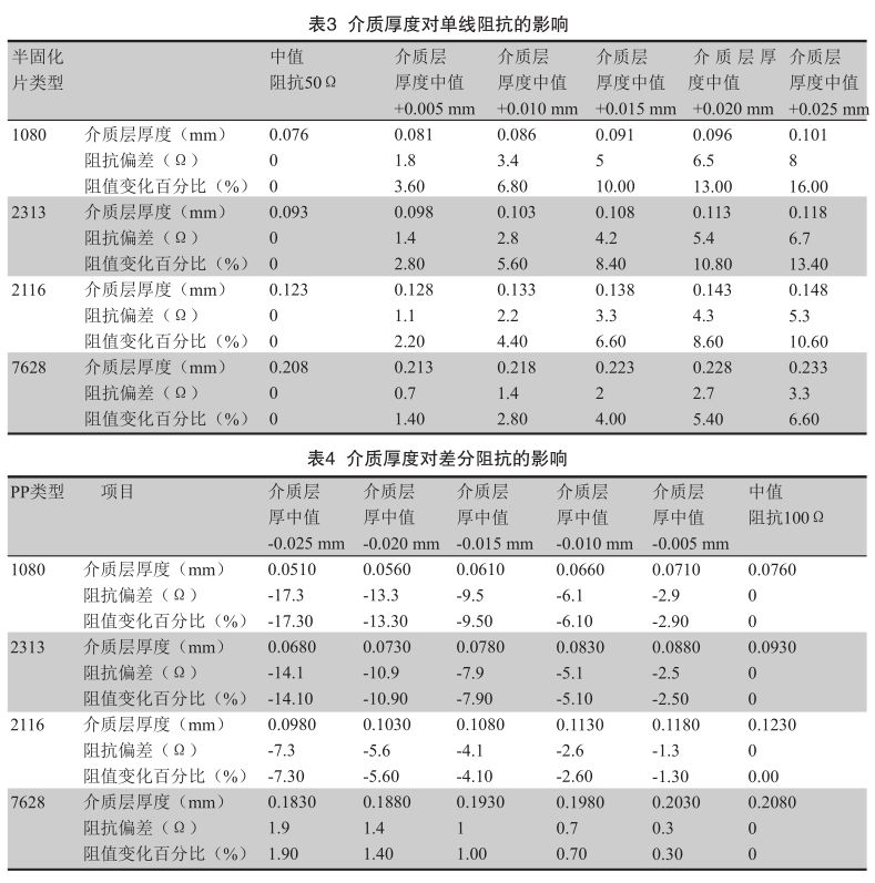
The thinner the dielectric layer thickness, the greater the impact of dielectric layer thickness fluctuations on the impedance line resistance; conversely, the thicker the dielectric layer thickness, the smaller the impact of dielectric layer thickness fluctuations on the impedance line resistance. Particularly, if a single sheet of 1080 or thinner semi-cured sheet is used as the reference layer for the impedance line’s corresponding dielectric layer, special attention must be paid to controlling the fluctuation range of this dielectric layer thickness.
2.3 The Impact of Different ε (Dielectric Constant) on Single Line Impedance and Differential Impedance
The impact of different dielectric constants of semi-cured sheets on impedance is analyzed, as shown in Tables 5 and 6.
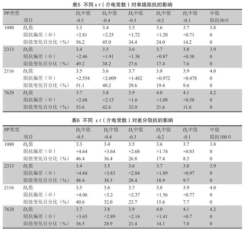
For every 0.1 change in dielectric constant, the impact on single line impedance resistance is approximately 10%; the impact on differential impedance resistance is approximately 8%.
2.4 The Impact of Dielectric Thickness Control on the Residual Copper Rate of Impedance Strips and Internal Impedance Control Areas
Dielectric thickness = semi-cured sheet thickness – copper thickness * (100% – residual copper rate), therefore, under the same semi-cured sheet structure, one of the main factors affecting the dielectric layer thickness is the residual copper rate, which is associated with the Gerber graphic design. Thus, it is essential to differentiate the residual copper rate at the location of the impedance line.
The following shows the impact of different residual copper rates on dielectric thickness. Taking the theoretical thickness of 0.083 mm for a 1080 semi-cured sheet and an inner layer copper thickness of 35 μm as an example, the impact of different residual copper rates on dielectric thickness is described in Table 7.
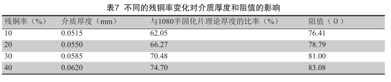
From Table 7, it can be seen that for every 10% change in residual copper rate, the dielectric thickness will change by 4.2%, and the impact on the impedance value for differential impedance line width/spacing (0.10 mm/0.152 mm) is 2.08~2.38 ohms. If the median impedance is 76 ohms, and the impedance tolerance is controlled at ±10% (7.6 ohms), then for every 10% change in residual copper rate, the contribution to the impedance value deviation is 26%~31%.
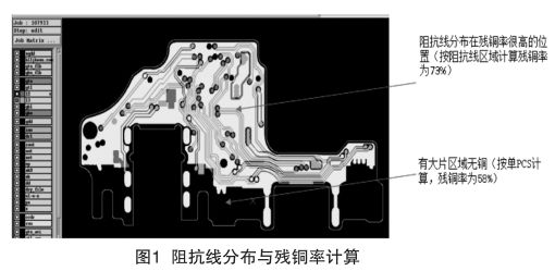
To ensure that the impedance values on the impedance test board (the CITS900S4 Polar Impedance Tester can only use dedicated test boards) are closer to the internal impedance values, the residual copper rate of the impedance test board should be kept consistent with that of the internal unit during engineering design. When the residual copper rates of the impedance test board and the internal unit differ by more than 5%, the impedance line width design on the test board and that of the internal unit should be produced separately. In situations like Figure 1, where the distribution of impedance lines is concerned, the residual copper rate cannot be calculated based on the entire area of the single piece, but should be calculated based on the copper surface area within the impedance line distribution region.
2.5 The Impact of Browning of Inner Layer Core Board on Impedance Values
To increase the bonding strength between the inner copper surface and the semi-cured sheet, the inner pattern must be browned or blackened before pressing. By micro-etching the copper surface, the impedance line will also undergo corresponding etching treatment, leading to a reduction in line width of 3 μm~5 μm before and after browning through slice analysis. For fine and dense impedance lines, the impact on impedance values is approximately 3.1Ω. The impact of micro-etching during browning accounts for more than 30% of the impedance tolerance, thus, during impedance line compensation, it is necessary to increase the browning compensation (usually 1/4 of the compensation value), and for an inner copper thickness of 35 mm, the normal compensation of 0.02 mm should be followed by an additional 0.005 mm compensation.
2.6 The Impact of Line Compensation on Impedance
Figure 2 shows the highlighted impedance line; if the compensation amount is applied uniformly across the board, due to its distribution in a relatively independent area, the etched board may easily exhibit local impedance line thinning issues, leading to locally increased impedance.
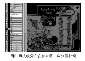
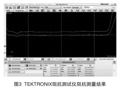
Figure 2 highlights the impedance line design with line width/spacing of 0.094 mm/0.109 mm, with a target controlled impedance value of (85±8.5)Ω. Using the TEKTRONIX impedance tester to measure this group of impedance lines within the board, the resistance values range from 91.25Ω to 95.5Ω, with the maximum value exceeding the impedance control specifications, and the fluctuation range of the impedance value is 4.25Ω, as shown in Figure 3.
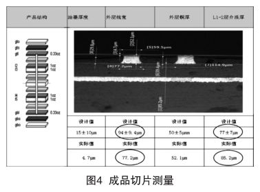
From the slice data (Figure 4) analysis, among the factors affecting impedance values, the outer layer line width exceeds the lower control limit, and the dielectric thickness exceeds the upper limit, while other potentially variable factors remain relatively stable. From the analysis of the factors affecting impedance, it can be concluded that the primary causes of increased impedance are the thinning of the lines and excessive dielectric layer thickness.
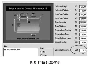
Substituting the outer layer slice data into the impedance calculation model, as shown in Figure 5. By conducting stratified analysis on the various factors affecting impedance, it can be observed that when the dielectric layer is very thin, the impact of line width on the resistance is significant. Therefore, during engineering design, different compensation should be applied for different impedance line widths, especially for dense areas, sparse areas, and independent areas, which should be compensated in segments. Even for the same group of lines or the same line, compensation should be differentiated according to their distribution areas on the PCB to minimize the fluctuation range of the impedance values.
2.7 Summary
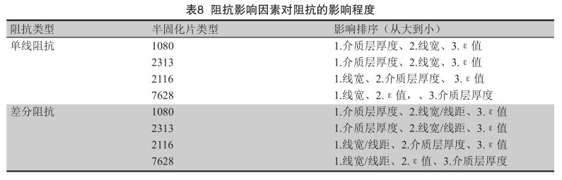
Through the aforementioned experiments and analyses, the main factors affecting PCB impedance and varying degrees of impedance influence are listed in Table 8.
3
Conclusion
Based on the above experiments and analyses, high precision impedance should be controlled according to the type of semi-cured sheets during design. The recommended control schemes are as follows:
(1) When the thickness of the semi-cured sheet is thinner, it is necessary to control the fluctuation range of the dielectric layer thickness, primarily determining the residual copper rate calculation based on the graphic distribution of the impedance lines.
(2) When the thickness of the semi-cured sheet is thinner, it is necessary to control the fluctuation range of the impedance line width, primarily determining the segmented compensation method based on the graphic distribution of the impedance lines. Additionally, for internal impedance, compensation should be applied to the line width based on the amount of micro-etching during the browning treatment.
(3) When the ε value deviates from the true ε value by 0.5, the impact on the tolerance range of the impedance value approaches 50%. Therefore, in actual production, ε values should be inferred based on actual production results, stabilizing the ε value within a fluctuation range of 0.1.
Author Introduction
Liao Minsheng, Harbin University of Science and Technology, majoring in Automation, Bachelor’s degree, Senior Engineer in the Engineering Department.
Zhang Baiyong, Liu Guangting: Jingwang Electronic Technology (Longchuan) Co., Ltd.
Source: “Printed Circuit Information” December issue
[Please indicate the source when reprinting]
*This journal is publicly distributed both domestically and internationally/monthly*
Subscription Methods:
1. Call 021-64139487-301 hotline to subscribe
2. Scan the QR code below to purchase online at the official WeChat store



January 16, 2019 WeChat Daily
Welcome to submit to: [email protected]
WeChat service hotline: 021-64139487-310 Mao Wenrui